Solved
STM32H7S78-DK — actual PCB stackup & Octo-SPI/Hexa-SPI impedance?
Hi all,
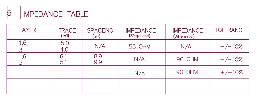
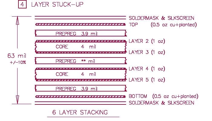
I'm reusing the STM32H7S78-DK's Octo-SPI flash (MX66UW1G45G) and Hexadeca-SPI PSRAM (APS256) sub-circuits on a custom board and want to match the DK's signal integrity. I can't find the fabrication stackup or impedance spec in the docs. Could ST share, for the DK (please confirm board rev):
- Full layer stackup — copper weights and each dielectric thickness/material.
- Target impedance (single-ended + any diff) and tolerance for the Octo-SPI / Hexa-SPI nets.
- Trace width/spacing for those buses, and their routing layer + reference plane.
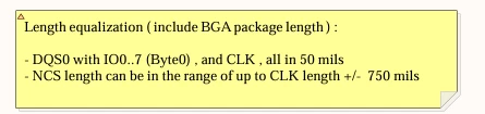
- Any length-matching constraints on those groups.
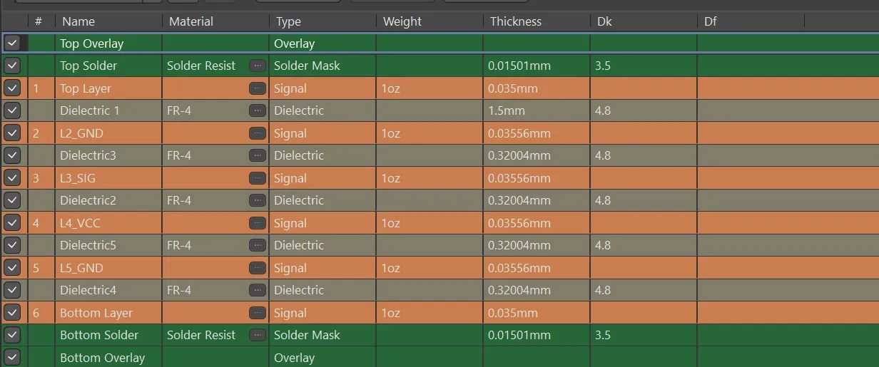
For reference, the published Altium reference-design project ships with an unconfigured stackup (single 1.5 mm dielectric, all layers typed Signal), so it doesn't reflect the real fabricated stack — which is why I'm asking for the actual values.
Thanks!