Associate II
July 4, 2026
Question

STM32H7B3I-DK C03– Clarification Regarding R114 Voltage Drop on 5V_VIN Input

  • July 4, 2026
  • 1 reply
  • 71 views


Dear STMicroelectronics Support,

In our application, the STM32H7B3I-DK board is used in a "shield" configuration: it is mounted on a carrier/daughter board(PHOTO 2) (via the Arduino connectors CN19/CN20/CN10/CN11) which supplies its power. The daughter board therefore injects a 5V voltage directly onto CN19, pin 1 (5V_VIN), without going through a USB supply or through the standard VIN input of the kit.

Power configuration

  • 5 V is applied to CN19, pin 1 (5V_VIN).
  • JP1 is configured in the 5V_VIN position.
  • VIN (CN19, pin 8) is left unconnected.
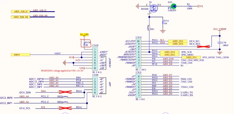
Measurements

  • Voltage before R114 (1 kΩ): 5.0 V
  • Voltage after R114: 1.6 V

This corresponds to a voltage drop of approximately 3.4 V across R114, which indicates a current of about 3.4 mA flowing through the resistor.

I would like to better understand whether this behavior is expected and the purpose of R114 in this circuit.

Could you please clarify the following points?

  1. Is this voltage drop across R114 normal when powering the board through 5V_VIN?
  2. What is the function of R114 in this design? Is it intended for current limiting, protection, or another purpose?
  3. Would it be safe to replace R114 (1 kΩ) with a 0 Ω resistor to eliminate this voltage drop, or could this affect the proper operation or protection of the board?

Thank you in advance for your assistance.

Kind regards,

1 reply

Mike_ST
ST Technical Moderator
July 6, 2026

Hello,

>> Is this voltage drop across R114 normal when powering the board through 5V_VIN?

If you’re trying to  power the boards with that pin, the voltage accross R114 drop is normal accross the 1K.

Originally this pin is not intented to power the board.

>> What is the function of R114 in this design? Is it intended for current limiting, protection, or another purpose?

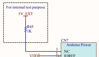
Testing purpose on ST board, pin 1 on this arduino is defined as NC.

Our latest designs include that note:

>> Would it be safe to replace R114 (1 kΩ) with a 0 Ω resistor to eliminate this voltage drop, or could this affect the proper operation or protection of the board?

You could try, but maybe there would be a problem with the U3 LDO, I have never tested..

I would prefer injecting 5V on CN19/Pin 5 while removing JP1.


In order to give better visibility on the answered topics, please click on 'Best answer' on the reply which solved your issue or answered your question. 
ARIJAuthor
Associate II
July 6, 2026

Hello,

Thank you for your clarification.

I have one additional question.

Would it be possible to power the board directly with 3.3 V through CN19 Pin 4 (3V3) instead of using the 5V pin 5? 

Thank you for your support.

Best regards,

Mike_ST
ST Technical Moderator
July 7, 2026

Hello,

The user manuel explicitly says that these are outputs:


But, that doesn’t mean I wouldn’t try. For instance If I would inject 3.3V on pin 4, at least would remove SB33 beforehand.

Maybe there is more to do, I didn’t check further.


Anyways, before doing anything, please check the documentation, to fully understand what is possible.

The user manual is here:

https://www.st.com/resource/en/user_manual/um2569-discovery-kit-with-stm32h7b3li-mcu-stmicroelectronics.pdf

And the schematic here:

https://www.st.com/en/evaluation-tools/stm32h7b3i-dk.html#cad-resources

In order to give better visibility on the answered topics, please click on 'Best answer' on the reply which solved your issue or answered your question.