


STM32F103RBT6, SPI and I2C conflict
Hello,
At present I trt o interface an SPI based SSD1309 Display and I2C based DS3231 RTC with STM32F103RBT6 using Nucleo board MB1136 F103RB C. For your reference I have attached screenshot of port assignment for those devices.
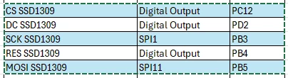
void Init_GPIOs(void) {
/* --- 1. Peripheral Clock Enable --- */
// Enable clocks for all GPIO ports and AFIO (Alternate Function I/O)
RCC->APB2ENR |= (RCC_APB2ENR_IOPAEN | RCC_APB2ENR_IOPBEN |
RCC_APB2ENR_IOPCEN | RCC_APB2ENR_IOPDEN |
RCC_APB2ENR_AFIOEN);
/* --- 2. Pin Remapping & JTAG Management --- */
// Disable JTAG/SWD remap to reclaim PB3, PB4, and PA15 for GPIO/Alternate Function usage
AFIO->MAPR &= ~AFIO_MAPR_SWJ_CFG;
AFIO->MAPR |= AFIO_MAPR_SWJ_CFG_JTAGDISABLE;
// Remap SPI1 to PB3/PB4/PB5 as per hardware design
AFIO->MAPR |= AFIO_MAPR_SPI1_REMAP;
/* --- 3. Initialize Display Control Pins (Soft-Step) --- */
// Configuring critical control pins first ensures the display state is stable
// before the high-speed SPI clock begins toggling.
GPIOB->CRL &= ~(0x000F0000U); GPIOB->CRL |= (0x00030000U); // PB4: Display Reset (Output)
GPIOC->CRH &= ~(0x000F0000U); GPIOC->CRH |= (0x00030000U); // PC12: Display CS (Output)
GPIOD->CRL &= ~(0x00000F00U); GPIOD->CRL |= (0x00000300U); // PD2: Display DC (Output)
/* --- 4. Initialize SPI Pins (PB3/PB5) --- */
// Set SPI1 SCK (PB3) and MOSI (PB5) to Alternate Function Output (50MHz)
GPIOB->CRL &= ~(0x00F0F000U);
GPIOB->CRL |= (0x00B0B000U);
/* --- 5. Port A Configuration (Sensors, RAK, UART1, Tacts, RS485 DE) --- */
// Configure PA0-PA4 (Sensors) as inputs, PA5 (LED), PA8 (Reset), PA15 (RS485 DE) as outputs.
// Configure UART1 (PA9/10) for RAK communication.
GPIOA->CRL &= ~(0xFFFFFFF0U); GPIOA->CRL |= (0x38888888U);
GPIOA->CRH &= ~(0xFF0F00FFU); GPIOA->CRH |= (0x34433443U);
// Explicitly set pull-downs for digital sensors
GPIOA->ODR &= ~(0x001FU);
/* --- 6. Port B Configuration (SPI, I2C1, I2C2, AC Sens, LEDs, RTC) --- */
// PB0 (EEPROM WP), PB1 (AC1), PB6/7 (I2C1), PB8 (RTC RST), PB9 (Tact),
// PB10/11 (I2C2), PB12/13 (AC Sens), PB14/15 (LEDs).
GPIOB->CRL &= ~(0xFF000000U); GPIOB->CRL |= (0xBB34BB33U);
GPIOB->CRH &= ~(0xFFFF000FU); GPIOB->CRH |= (0xBB3333BBU);
// Enable internal pull-ups for I2C1 (RTC) lines
GPIOB->ODR |= (GPIO_ODR_ODR6 | GPIO_ODR_ODR7);
/* --- 7. Port C Configuration (Analog, LEDs, UART3, CS, Sensors) --- */
// PC0-PC3 (Analog Sensors), PC4 (Relay), PC5 (AC Meas), PC6-PC9 (Status LEDs),
// PC10/11 (UART3 RS485), PC13-15 (Digital Sensors).
GPIOC->CRL &= ~(0xFF00FFFFU); GPIOC->CRL |= (0x33040000U);
GPIOC->CRH &= ~(0xFFF000FFU); GPIOC->CRH |= (0x8883B333U);
// Force PC13-PC15 to pull-down mode for digital sensors
GPIOC->ODR &= ~(GPIO_ODR_ODR13 | GPIO_ODR_ODR14 | GPIO_ODR_ODR15);
}
This is my SSD1309 Display Initilization code
void Init_SSD1309Disp(void) {
// Force reset pin LOW (Active Reset)
GPIOB->BRR = SSD1309_DISP_RES_PIN;
BlockDelay_ms(100);
// Force reset pin HIGH (Active Operating Mode)
GPIOB->BSRR = SSD1309_DISP_RES_PIN;
BlockDelay_ms(100);
// Send standard initialization commands
Cmd_To_SSD1309(0xAE); Cmd_To_SSD1309(0xD5); Cmd_To_SSD1309(0x80);
Cmd_To_SSD1309(0xA8); Cmd_To_SSD1309(0x3F); Cmd_To_SSD1309(0xD3);
Cmd_To_SSD1309(0x00); Cmd_To_SSD1309(0x40); Cmd_To_SSD1309(0x8D);
Cmd_To_SSD1309(0x14); Cmd_To_SSD1309(0xA1); Cmd_To_SSD1309(0xC8);
Cmd_To_SSD1309(0xDA); Cmd_To_SSD1309(0x12); Cmd_To_SSD1309(0x81);
Cmd_To_SSD1309(0x7F); Cmd_To_SSD1309(0x20); Cmd_To_SSD1309(0x02);
Cmd_To_SSD1309(0xAF);
}
Funtion required for SSD1309
void Cmd_To_SSD1309(uint8_t cmd) {
GPIOC->BRR = SSD1309_DISP_CS_PIN;
GPIOD->BRR = SSD1309_DISP_DC_PIN;
Send_SPI_Char(cmd);
GPIOC->BSRR = SSD1309_DISP_CS_PIN;
}
Funtion required for SSD1309
void Send_SPI_Char(uint8_t data) {
/* Wait for the transmit buffer to be empty before loading the data register */
while (!(SPI1->SR & SPI_SR_TXE));
/* Load the data byte into the SPI data register */
SPI1->DR = data;
/* Block until the internal SPI shift register has finished the transaction */
while (SPI1->SR & SPI_SR_BSY);
}
With further functions I am able to make the Display work as I needed.
Then I tried to impelment I2C for DS3231.
void Init_RTC_I2C(void) {
// 1. Force pins to Input-Floating to prevent driver conflict
GPIOB->CRL &= ~(0xFF000000U);
// 2. Enable Clock
RCC->APB1ENR |= RCC_APB1ENR_I2C1EN;
// 3. Configure peripheral (already tested as working without reset)
I2C1->CR1 &= ~I2C_CR1_PE;
I2C1->CR2 = (I2C1_PCLK1_MHZ & I2C_CR2_FREQ);
// ... [timing setup] ...
I2C1->CR1 |= I2C_CR1_PE;
// 4. Finally, set pins to AF Open-Drain for I2C usage
GPIOB->CRL |= 0xFF000000U;
}
When Clock is enabled by “RCC->APB1ENR |= RCC_APB1ENR_I2C1EN;” the SSD1309 is currupted.
The sequence I call these functions are as
int main(void) {
// 1. Core Config
// 1. System Config
Config_48MHz_HSI();
// 2. Setup Pins
Init_GPIOs();
// 3. Initialize I2C independently
Init_RTC_I2C();
BlockDelay_ms(20); // Essential: Give the I2C bus time to stabilize after SWRST
// 4. Initialize other peripherals
Init_LEDs();
Init_SPI();
Init_Timer4_1msISR();
Init_ADC_DMA();
// 5. Display Initialization (Must be last)
Init_SSD1309Disp();
Am I missing anything fundametally? I have completed my PCB layouting with these port assignment. Now I am bit nervious.
Please help me to identify the problem.
Thank you,
With best ragrds,
Anesh S.

