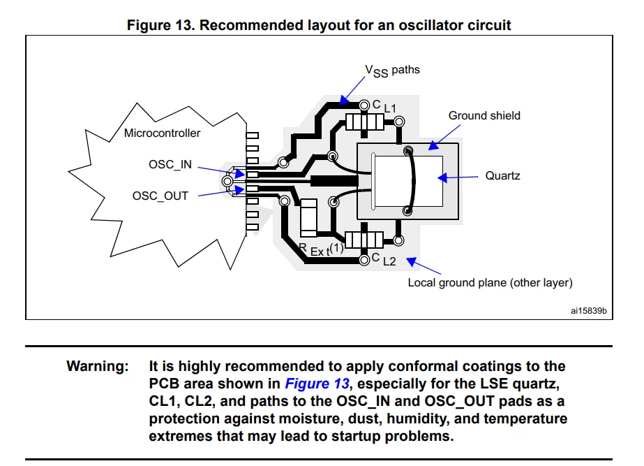
problem is with placing the crystal on the PCB design.
Hi
,
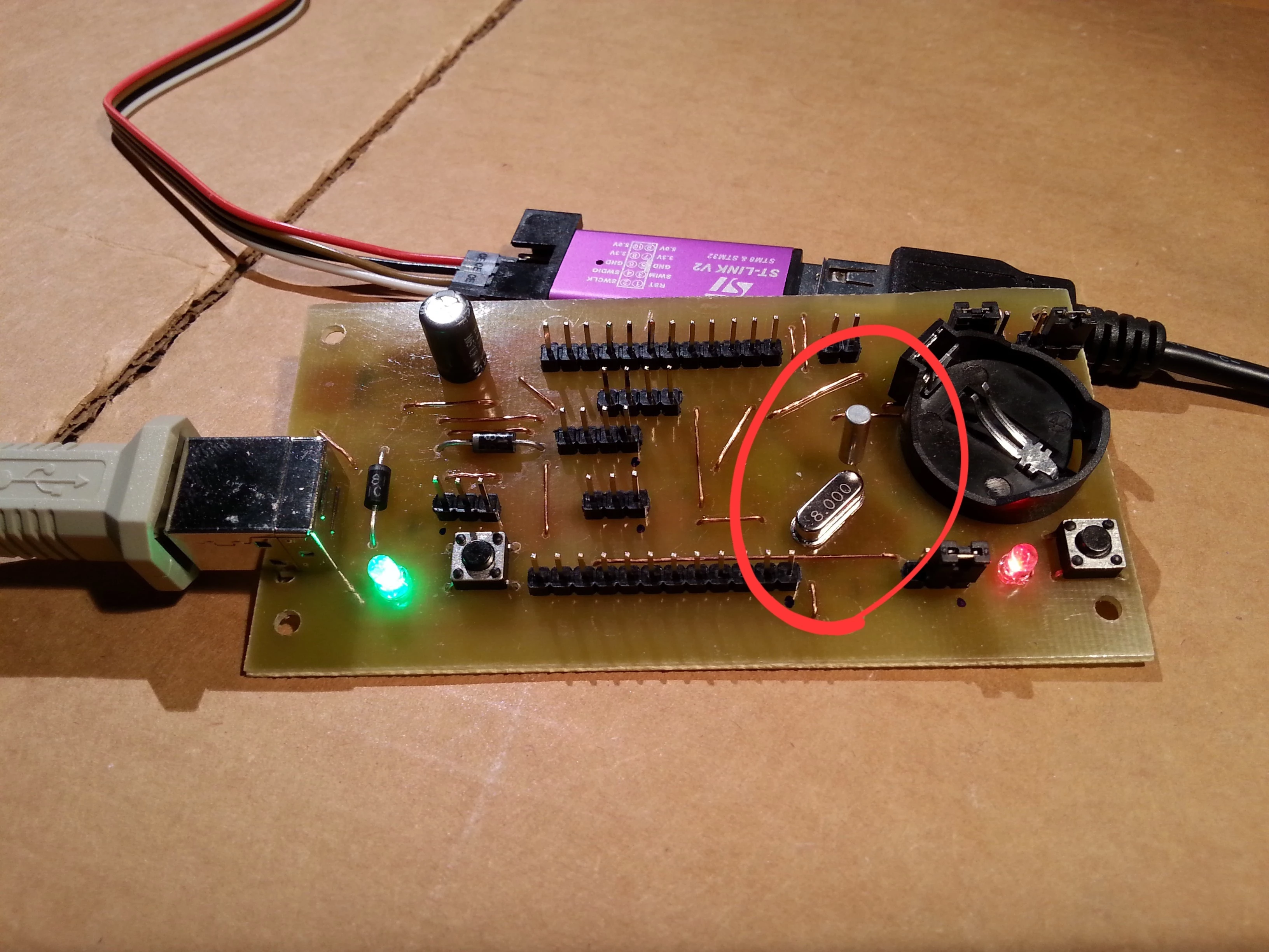
I'm new to PCB design. I'm planning to build a handmade board for a project that uses the STM32F103C8T6, and I've run into some issues in certain parts of the PCB design. My board only has copper on one side (single-sided). For the HSE 8MHz and LSE 32.768kHz crystal oscillators, the body needs to be placed on the bottom layer, with the pins passing through holes to reach the top layer where they will be soldered.
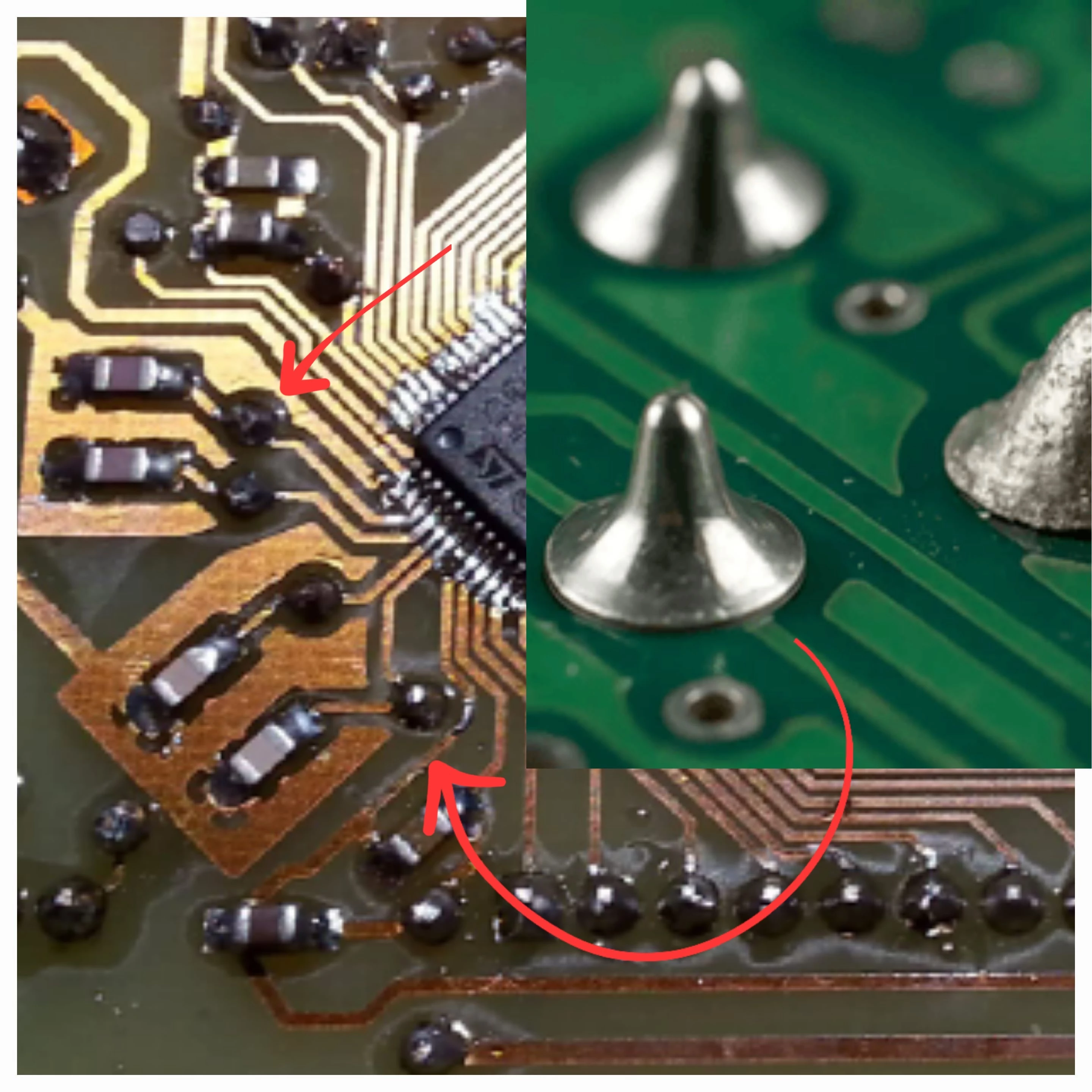
I'm concerned about the soldered area where the solder forms a fillet on the top layer, and whether this fillet, being in line with the OSC traces running toward the MCU, could cause problems.
To put it simply: could the solder fillet of the crystal on the top layer cause frequency issues, reduced performance, or make it completely unusable?
Since my project is currently in the experimental stage, I haven't built the board yet. The images I've included are just for better understanding and were collected from a few websites.
What's your opinion on this?