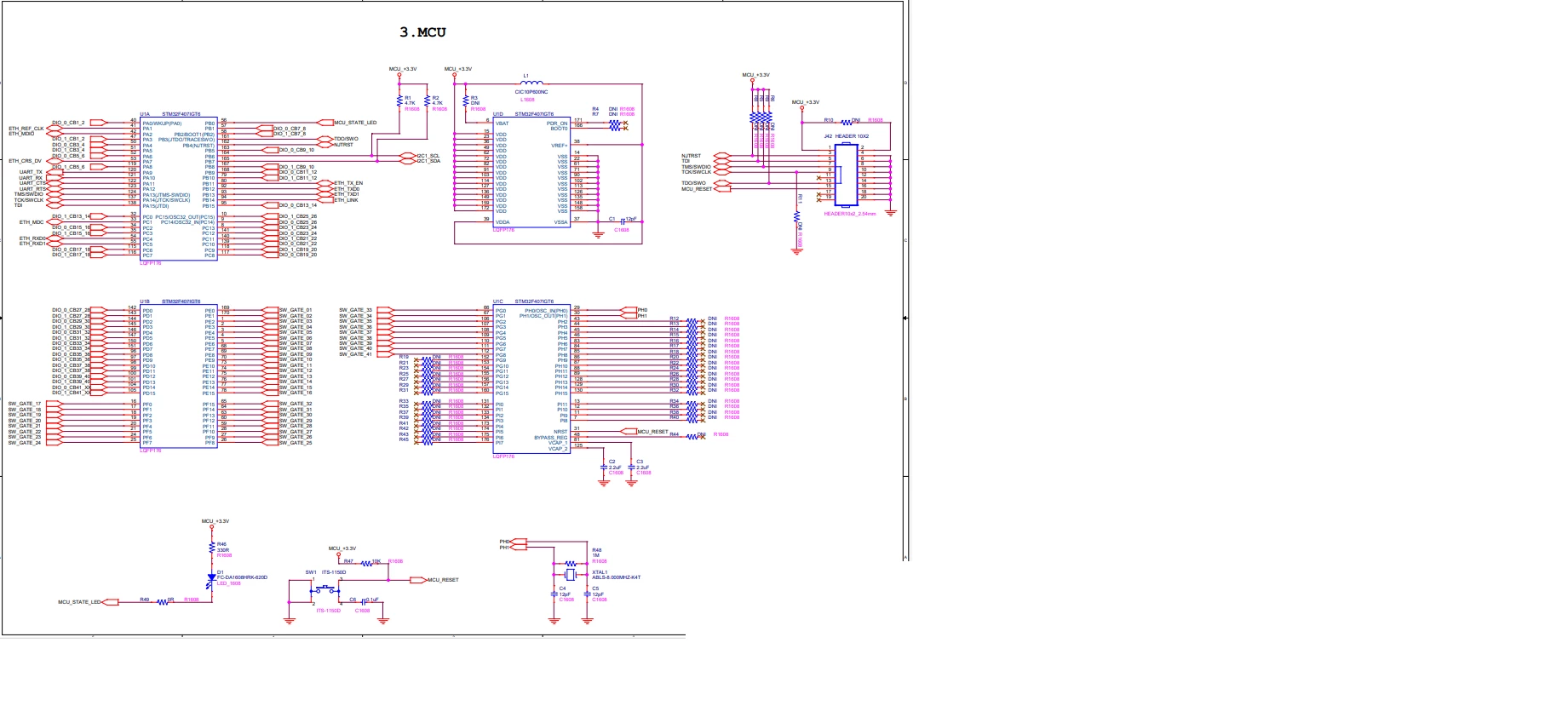
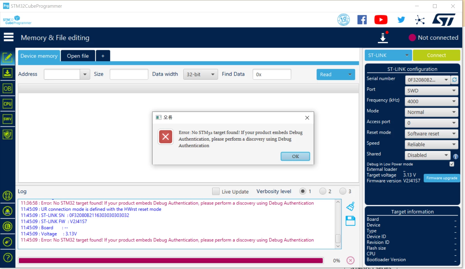
I am using the STM32F407IGT6 chip. However, when I connected JTAG, the symptoms shown in the picture appear. So I have completed the VDD or continuity test. Can you tell me the circuit diagram and the reason?
the pull resistor at BOOT0 have to be connected to GND instead of VDD.
BTW: the pull-up at NRST is not necessary, see the description of NRST in the respective reference manual.
Hope that helps?
Regards /Peter
In order to give better visibility on the answered topics, please click on Accept as Solution on the reply which solved your issue or answered your question.
I tried connecting BOOT0 to nothing or connecting it to GND. NRST(R8) is not connected to anything other than a pull-up resistor. Still not working. Do you know why? Boot1 is currently in a null state with nothing connected.