
Associate II
October 10, 2026
Question

Clarification needed: in UM2408 (Section 7.12 Note 3) regarding Ethernet PHY SB13 on NUCLEO-H755ZI-Q (MB1363)

  • October 10, 2026
  • 7 replies
  • 152 views

Hi ST Community & Support Team,

I am working with the NUCLEO-H755ZI-Q (Board MB1363) and I noticed a potential typo in the User Manual UM2408 (Rev 6). 31/57

In Section 7.12 - Ethernet, Note 3 states:

"On MB1363 Rev.C: Ethernet PHY LAN8742A must be set in the Power-down mode [...] SB13 can also be removed to get the same effect."

However, when checking the schematic (mb1363-h755ziq-d01_schematic.pdf), SB13 is actually located in the ST-LINK Virtual COM Port level translator circuit (U1: SN74LVC2T45DCUT) between STLK_VCP_RX and T_VCP_TX, and is already marked as DNF (Do Not Fit).

It seems SB13 in Note 3 is a documentation typo pointing to the wrong solder bridge.

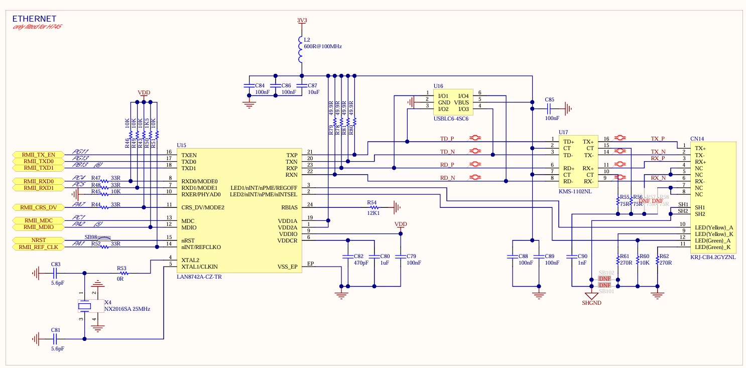
Based on the schematic, there is no dedicated hardware jumper or solder bridge (SB) to physically disconnect the power or clock lines of the LAN8742A PHY.

Furthermore, upon a detailed review of the schematic, there is no dedicated hardware jumper or solder bridge (SB) to physically disconnect the power or clock lines of the LAN8742A PHY to achieve a hardware power-down state.

This raises a few crucial concerns for custom hardware implementations where these pins need to be repurposed:

  1. Since no hardware disconnect jumper exists, is putting the PHY into low-power mode strictly handled through software (setting bit 11 in the Basic Control Register at address 0x00 via MDIO)?

  2. If the Ethernet pins on the MCU are repurposed for other peripherals (e.g., custom FPGA communication), does leaving the LAN8742A powered on its main VDD lines while its digital control/data lines are left floating or driven externally risk causing parasitic powering, leakage current, or signal contention issues?

  3. Could you please clarify the correct documentation/procedure and confirm if this typo in UM2408 will be fixed in a future revision?
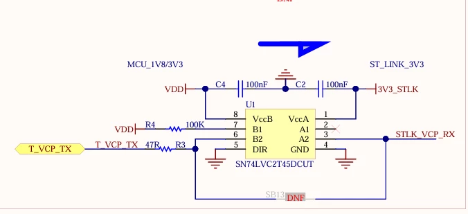


Schematic diagram of the ST-LINK Virtual COM Port level translator circuit (U1: SN74LVC2T45DCUT) highlighting the position of solder bridge SB13 (marked DNF).


Schematic diagram of the Ethernet section (LAN8742A PHY) on the NUCLEO-H755ZI-Q board.


Thank you for your help!

7 replies

Associate II
October 10, 2026

Following this logic, if we simply remove the signal solder bridges (SB80, SB48, SB63, etc.) according to Table 14 to isolate the MCU, the LAN8742A remains fully powered on its main VDD lines with all its digital control and data inputs left completely uncommitted and floating. In CMOS architecture, doesn't leaving input pins floating while the power rail is active risk causing severe internal cross-conduction, unpredictable leakage currents, or eventual thermal degradation inside the PHY? Furthermore, with the PHY still running, won't its internal 50 MHz oscillator continue to drive an un-terminated RMII_REF_CLK signal into an open trace, potentially creating significant high-frequency noise and electromagnetic interference across the board?

To mitigate these risks and safely neutralize the chip, this leaves us with exactly two potential correction paths—either via software control or a permanent physical modification. The software route would require keeping the MDIO/MDC lines temporarily connected to execute an initial startup code that sets bit 11 of the Basic Control Register to force a low-power state before reconfiguring the MCU pins. Alternatively, the physical approach would involve forcing a permanent hardware reset by opening SB98 and tying the PHY’s nRST pin (Pin 15) directly to Ground (GND). Theoretically, tying nRST to GND should keep the internal logic frozen, shut down the 50 MHz clock output, and force all remaining floating IO pins into a safe, high-impedance state without needing to physically desolder the entire QFN package.

Associate II
October 10, 2026

Following my own analysis, I would not suggest relying on the software workaround as a clean or reliable long-term alternative. Even if we configure the MCU dynamically to disable the PHY via MDIO right after boot, the 50 MHz oscillator will still kick in during the critical first milliseconds of the power-up phase. Driving a high-frequency square wave into open, un-terminated traces (since the signal Solder Bridges are removed) will inevitably create signal reflections, impedance mismatches, and radiate electromagnetic interference (EMI) into neighboring traces during startup. For applications with strict signal integrity requirements where these pins interface with an external FPGA, shouldn't a temporary "glitch clock" at boot be completely avoided, and does this mean a definitive hardware isolation approach is theoretically more appropriate?

Associate II
October 10, 2026

As an update, I looked into the Microchip LAN8742A-CZ-TR datasheet and schematic. It appears that keeping the nRST pin (Pin 15) tied permanently to Ground (GND) is a viable solution, as a hardware reset forces all digital RMII outputs into a true high-impedance (tri-state) mode while shutting down the internal clock. Furthermore, since most of the critical RMII lines on the MB1363 board already include 10kΩ pull-up restoration resistors, my previous concerns about uncommitted floating lines causing internal CMOS cross-conduction might be incorrect.

Could you please confirm if holding nRST permanently LOW (by opening SB98 and tying the PHY side to GND) is fully supported and safe for long-term operation? Will the presence of the onboard 10kΩ pull-up resistors cause any unexpected current leakage or conflict with the MCU/FPGA lines when the PHY is held in this permanent hardware reset state?

LCE
Principal III
October 10, 2026

I don’t know this particular Nucleo, but usually each signal line to the PHY has either a solder bridge, a series resistor, or a jumper.

Check this on your board, then remove these for all the GPIOs you need.

Visitor
October 10, 2026

William,

I think SB13 in UM2408 is a documentation typo, maybe a copy-paste mistake. You can find similar description in the other user manual and schematic. Its original purpose is to meter current consumption of STM32. It says so “To get a correct current consumption, the Ethernet PHY must be set in power-down mode or SB13 must be removed. Refer to Section 7.11: Ethernet for details”. SB13 is a solder bridge between PA1 of STM32 and RMII Reference Clock of LAN8742A. Removing SB13 is for metering current consumption of STM32 system, not for powering down PHY.

Back to questions.

Q1. Putting LAN8742A into power-down mode has two ways, setting bit 11 in the Basic Control Register or strap MODE[2:0]  pins to power-down mode during reset.

Q2. Force LAN8742A stayed on reset state, or remove jumpers/solder bridges between those pins you desire to use.

Q3. …depend on ST...

Associate II
October 10, 2026

1. The note explicitly mentions MB1363 Rev.C, but the NUCLEO-H755ZI-Q actually uses the MB1363 Rev.D-01 board revision 


According to the Document Revision History (Table 22), Rev.D specifically introduced layout modifications to correct the IDD current measurement issues. This perfectly matches the historical context provided earlier regarding old current metering workarounds.

2. Furthermore, the Ethernet schematic sheet for this family contains the hardware note: "ETHERNET only fitted for H745".

This suggests that the Ethernet block (marked “ETHERNET only fitted for H745” on the schematic) and the related documentation notes may have been originally written for the NUCLEO-H745ZI-Q and then shared with the H755ZI-Q user manual, possibly without updating the solder bridge references (such as SB13).

Could ST please clarify how the Ethernet PHY isolation procedure changes now that we are on Rev.D-01 instead of Rev.C, and confirm if forcing nRST low remains the only valid option for the H755 variant?

Explorer
October 10, 2026

wait for ST’s confirmation before tying nRST permanently to GND, since the PHY’s reset behavior and long-term safety need to be verified against the datasheet.
