

HMüll.4
Senior
May 19, 2022
Solved

Can't connect to J-Link debugger / Nucleo 466

I'm trying to run/debug my code on a Nucleo with STM32F466 via the SWD interface using a J-Link debugger. Unfortunately this always ends up with a message

Could not connect to target.

Please check power, connection and settings.

Trying to connect to the debugger/the board using an other IDE brings up some more information: here I'm getting an error message of the target having no power.

Now when I measure the SWD-interface (CN4), I find the error message is correct: there is no power at the CN4-pins 1 (VDD) and 3 (GND). So what is missing here? Do I need to set one of the jumpers to get the SWD interface powered properly?

As described in the manual, the two jumpers at CNs have been removed, the Nucelo-board itself is powered via USB.

This topic has been closed for replies.
Tesla DeLorean
Tesla DeLoreanBest answer
Guru
May 19, 2022

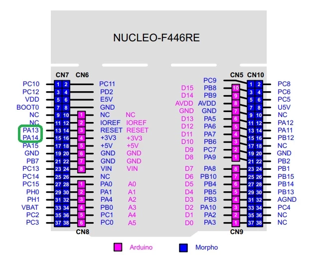
>> I can't find the signals for SWDIO and SWDCLK

Look for PA13 PA14, but as I said should be able to probe to the CN2 header

0693W00000NqHfgQAF.jpg

Tips, Buy me a coffee, or three.. PayPal Venmo (See Profile) Up vote any posts that you find helpful, it shows what's working..

10 replies

Andrew Neil
Super User
May 19, 2022

The J-Link also needs a "target voltage" reference connection. And, of course, GND.

0693W00000NqH46QAF.png 

https://wiki.segger.com/UM08001_J-Link_/_J-Trace_User_Guide#Reference_voltage_.28VTref.29

https://wiki.segger.com/UM08001_J-Link_/_J-Trace_User_Guide#Target_board_design_2

Also Take a look at the Nucleo schematics.

Note that you can convert the on-board ST-Link to a J-Link:

https://www.segger.com/products/debug-probes/j-link/models/other-j-links/st-link-on-board/

A complex system that works is invariably found to have evolved from a simple system that worked.A complex system designed from scratch never works and cannot be patched up to make it work.
HMüll.4
HMüll.4Author
Senior
May 19, 2022

Yes, GND is connected. According to the pinout of the Nucleo's SWD-connector I have connected VDD (1), SWCLK (2), GND (3), SWDIO(4), and RESET (5). Here "VDD" should be what you name "target voltage" - but the target does not provide that voltage. Exactly this is my problem!

Bob S
Super User
May 19, 2022

Are trying to connect the JLink to the 6-pin SIP header on the NUCLEO board? That connector is really meant for the NUCLEO's on-board STLink to control off-board devices, not for an external debugger to debug the on-board STM32.

If you like the JLink interface/features more then STLink, follow the link @Andrew Neil​ gave you to convert the onboard STLink to a (mostly) JLink.

But if you really need to use your stand-alone JLink - you will need to force the on-board STLink CPU to be held in reset (check your NUCLEO schematic, on the 144-pin NUCLEO boards this is SB107). Then you will need to get 3.3V for the JLink's VDD pin from one of the other headers

HMüll.4
HMüll.4Author
Senior
May 19, 2022

Qucik update: I found the 3.3V are at pin 5 of the CN4/SWD connector - not at pin 1. So...anybody an idea where I can get the correct manual/pinout from?

Bob S
Super User
May 19, 2022

That is NOT a 3.3V supply. That is the NRST signal that just HAPPENS to be at 3.3V. Go on ST's site, search for your board (NUCLEO-F446RE I presume). Click on the "CAD Resources" tab and download the schematic.

HMüll.4
HMüll.4Author
Senior
May 19, 2022

OK, I'm confused. What I'm referring to is this page out of the manual:

0693W00000NqHaqQAF.pngThere I can find the pinout of this SWD-connector with VDD (documented but missing), SWCLK, GND, SWDIO, NRST. Thats exactly the pinout which is expected/used by the J-Link debugger.

On the other hand: the pins 1, 7, 9, 13, 15 and 20 of Neils image refer to what connector of the Nucleo? The ST morpho connector pinout does not fit (and while VDD, GND and RESET are there at some other pins, I can't find the signals for SWDIO and SWDCLK).

Tesla DeLorean
Guru
May 19, 2022

CN4 is an OUTPUT connector for the on-board ST-LINK/V2-1 (STM32F103).

You need to get to the SWD signals of the STM32F446, the SWDIO/SWCLK will be exposed on one side of the CN2 jumpers.

Tips, Buy me a coffee, or three.. PayPal Venmo (See Profile) Up vote any posts that you find helpful, it shows what's working..
HMüll.4
HMüll.4Author
Senior
May 19, 2022

Who the fu** is designing such a poor board? So I have to collect the signals anywhere at the board? SWD/SWCLK at the CN2 connector (which pins?), GND and RESET at CN4 (or somewhere else?), VDD at wherever I find it?
