STM32 QSPI interface addressing in Dual-Flash memory mode
This article covers the following frequently asked question:
Why does the STM32 QSPI interface in Dual-Flash memory mode send addresses shifted right by 1 bit?
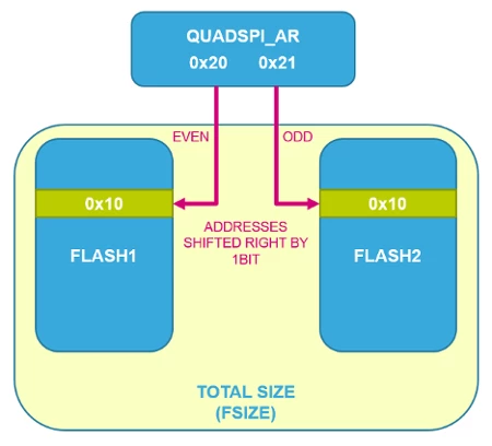
The configured address in the QUADSPI_AR is divided by 2 (shifted right by 1bit) in the Dual-Flash memory mode. This is because each connected memory bank represents half of the total size set in the FSIZE field. When writing or reading data, the QSPI peripheral uses the LSB for selecting between the two banks, and the rest of the SW-configured address for actually addressing the memory.
The LSB bit of address represents a specific flash:
- Even addresses are stored in Flash 1
- Odd addresses are stored in Flash 2
As an example, accesses to addresses "0x20" and "0x21" are demonstrated in the graphic below: