


How to implement the GPDMA hardware block request feature using LPTIM in STM32H563
Summary
This article presents a step-by-step tutorial on how to create an application developed on LPTIM and GPDMA hardware block request feature in the STM32H563 microcontroller. This tutorial is based on NUCLEO-H563ZI and can be easily tailored to any product that also implements the LPTIM BREQ feature.
Introduction
If you want to implement the GPDMA hardware block request feature on the STM32H563 microcontroller or any other controller that supports this feature using LPTIM, this article is for you.
The following software versions were used to build this tutorial:
Table of contents
1. Defining a hardware block request feature
The LPTIM update-event DMA request is a GPDMA block request used to update PWM-related timer registers in a single hardware-triggered transaction. When enabled, it allows the DMA to perform up to three single writes to the low-power timer. It targets up to two of LPTIMx_CCR1, LPTIMx_CCR2, and LPTIMx_RCR, followed by a mandatory write to LPTIMx_ARR to update the PWM period.
This mechanism relies on a dedicated hardware request connection between the LPTIM and the GPDMA, typically configured with BREQ = 1 and SWREQ = 0 in the selected GPDMA channel. In this mode, the request is handled at block level, meaning one LPTIM update event can trigger the complete register update sequence without CPU intervention.
To support this block-based transfer pattern, a 2D-capable GPDMA channel is used. CxBR1 defines the block-repeat count and direction, and CxBR2 defines the source and destination address offsets used to step through the register sequence.
Brief explanation of BREQ and SWREQ
- BREQ = 0: The hardware request is handled at the burst level.
- BREQ = 1: The hardware request is handled at the block level.
So, for LPTIM HRWBREQ, BREQ = 1 means that the peripheral request is consumed once per complete block transfer, not once per burst.
- SWREQ = 1: The channel is started by a software request for memory-to-memory use.
- SWREQ = 0: The channel is not in software-request mode, so the hardware request path is active.
In other words, for this use case, SWREQ must be 0 so the LPTIM hardware event can drive the GPDMA transfer.
Below is a simple diagram that explains the process:

2. Development
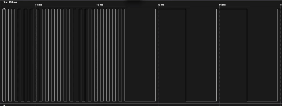
The purpose of this project is to create an LPTIM PWM signal on channel 2 that starts with a 100 µs period with a 50% duty cycle. After one second, we use the LPTIM hardware block request feature to modify the CCR2 register and then the ARR register to change the period to 1 ms with keeping a 50% duty cycle. This process is used to demonstrate the changes in the PWM signal.
2.1 Project configuration
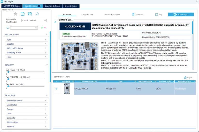
Start by creating a new project using the STM32CubeMX by clicking [File -> New -> STM32 Project]. Use the [Board Selector] tab and select the [Nucleo-H563].
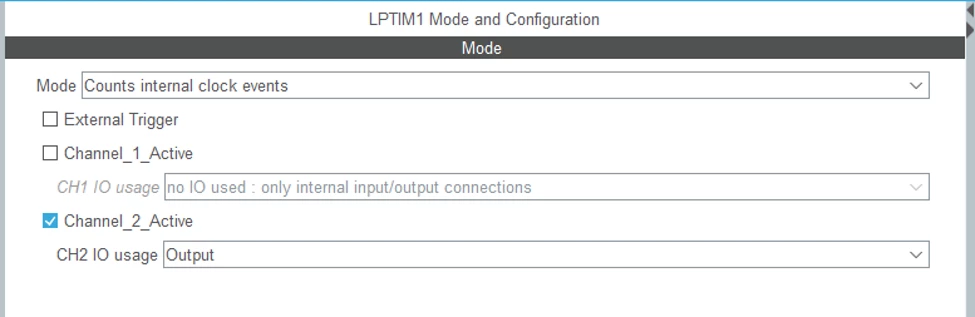
Once the project creation is done, enable LPTIM1 by selecting counts internal trigger mode and enable a second channel with CH2 I/O usage as output.
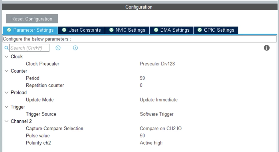
In the “Parameter Settings”, select Prescaler Div128.
Set the “Period” to 99.
Set the “Pulse Value” to 50.
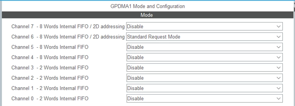
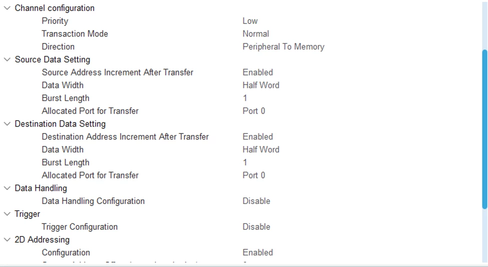
- In GPDMA1 under “system core”, enable Channel 6 as the “Standard Request Mode”.
- Under Request Configuration, set “Request” to “LPTIM1_UE”.
- Under Channel Configuration, set “Peripheral to Memory” to “Direction”.
- Under Source Data Setting, set “Source Address Increment After Transfer” to “Enabled”. Set the “Data Width” to “Half Word”.
- Under Destination Data Setting, set “Destination Address Increment After Transfer” to “Enabled”.
- Set the “Data Width” to “Half Word”.
- Finally, set 2D Addressing to “Enabled”.

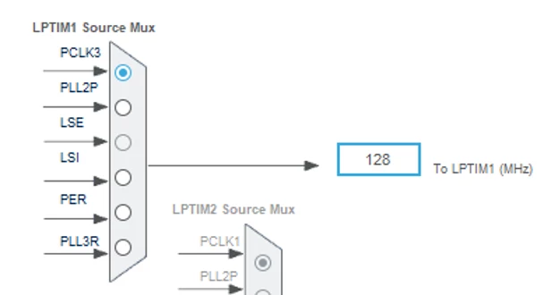
In clock configuration, ensure that LPTIM1 is at 128 MHz so it aligns with the selected prescaler value.
Name the project and generate the code.

In this example, we use direct register access to explain the utility of each line.
In main.c, add these code sections:
/* USER CODE BEGIN PV */
static uint16_t NewValues[2] = {500, 999};

/* USER CODE END PV */
/* USER CODE BEGIN 2 */
* Start PWM on LPTIM channel 2 with interrupt support */ HAL_LPTIM_PWM_Start_IT(&hlptim1, LPTIM_CHANNEL_2);
/* wait 1 second before applying the DMA update to visualize the changes */
HAL_Delay(1000);
/* configure the GPDMA block-repeat/direction control register (CBR1) * - clear the selected bits first * - set DDEC = 1 so the destination address is updated by decrementing * the programmed offset instead of incrementing it */
MODIFY_REG(GPDMA1_Channel6->CBR1,
DMA_CBR1_DDEC | DMA_CBR1_SDEC |
DMA_CBR1_BRDDEC | DMA_CBR1_BRSDEC |
DMA_CBR1_BRC,
DMA_CBR1_DDEC); /* DDEC = 1 */
/* configure the GPDMA transfer register (CTR3) * - set the destination address offset * - set the source address offset * - here the destination offset is programmed for a backward step */
MODIFY_REG(GPDMA1_Channel6->CTR3,DMA_CTR3_DAO | DMA_CTR3_SAO,(0x1EU << DMA_CTR3_DAO_Pos)); /* backward step */
* Start a DMA transfer: * - source: buffer NewValues in memory * - destination: LPTIM1 CCR2 register * - length: 4 transfers */
if (HAL_DMA_Start(&handle_GPDMA1_Channel6,
(uint32_t)NewValues,
(uint32_t)&LPTIM1->CCR2,
4U) != HAL_OK)
{
Error_Handler();
}
* Enable the LPTIM update-event DMA request: * the DMA transfer will be triggered by the next LPTIM update event */
__HAL_LPTIM_ENABLE_DMA(&hlptim1, LPTIM_DMA_UPDATE);
/* USER CODE END 2 */3. Results
If a logic analyzer or an oscilloscope is used to visualize the signal, both CCR and ARR change during a single synchronized DMA event. In this case, the signal from PG14 can be visualized.
By opening the memory map view, it is possible to observe that before calling:
__HAL_LPTIM_ENABLE_DMA(&hlptim1, LPTIM_DMA_UPDATE);LPTIM1_CCR2 (address 0x44004434) and LPTIM1_ARR (address 0x44004418) hold the values 0x63 and 0x32, which are equivalent to 99 and 50 in decimal, respectively.

After calling:
__HAL_LPTIM_ENABLE_DMA(&hlptim1, LPTIM_DMA_UPDATE);LPTIM1_CCR2 holds the value 0x1F4, which is equivalent to 500 in decimal, and LPTIM1_ARR holds the value 0x3E7, which is equivalent to 999 in decimal.

Conclusion
That concludes our article. Now, you have the needed information to implement the GPDMA hardware block request feature using LPTIM in STM32H563.
We hope this article was helpful!