ST25R500 Unexpected Reading Distance Results
Help Needed: ST25R500 Antenna Matching and Unexpected Reading Distance Results
Hello everyone,
Thank you for taking the time to read my post.
I am currently using the ST25R500 and designing a reader with the goal of achieving the maximum possible reading distance. I have been working on the antenna design, impedance matching, and the internal transmitter impedance settings of the ST25R500, but I have encountered some confusing results and would really appreciate your advice.
My antenna is a 2-turn enamelled-wire coil. For the impedance matching, I am using the impedance matching software officially recommended by ST.
Based on the recommendations in the datasheet, I set my target impedance to:
10 Ω − j4 Ω
As far as I understand, this target impedance should be within the recommended range.
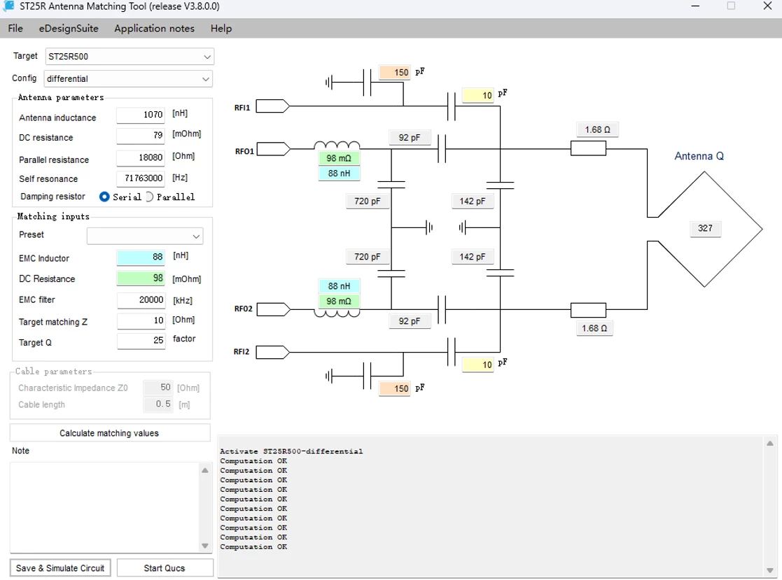
I entered my antenna parameters into the official matching software and used its built-in simulator. I then adjusted the values of the matching components, as shown in Figures 1 and 2.
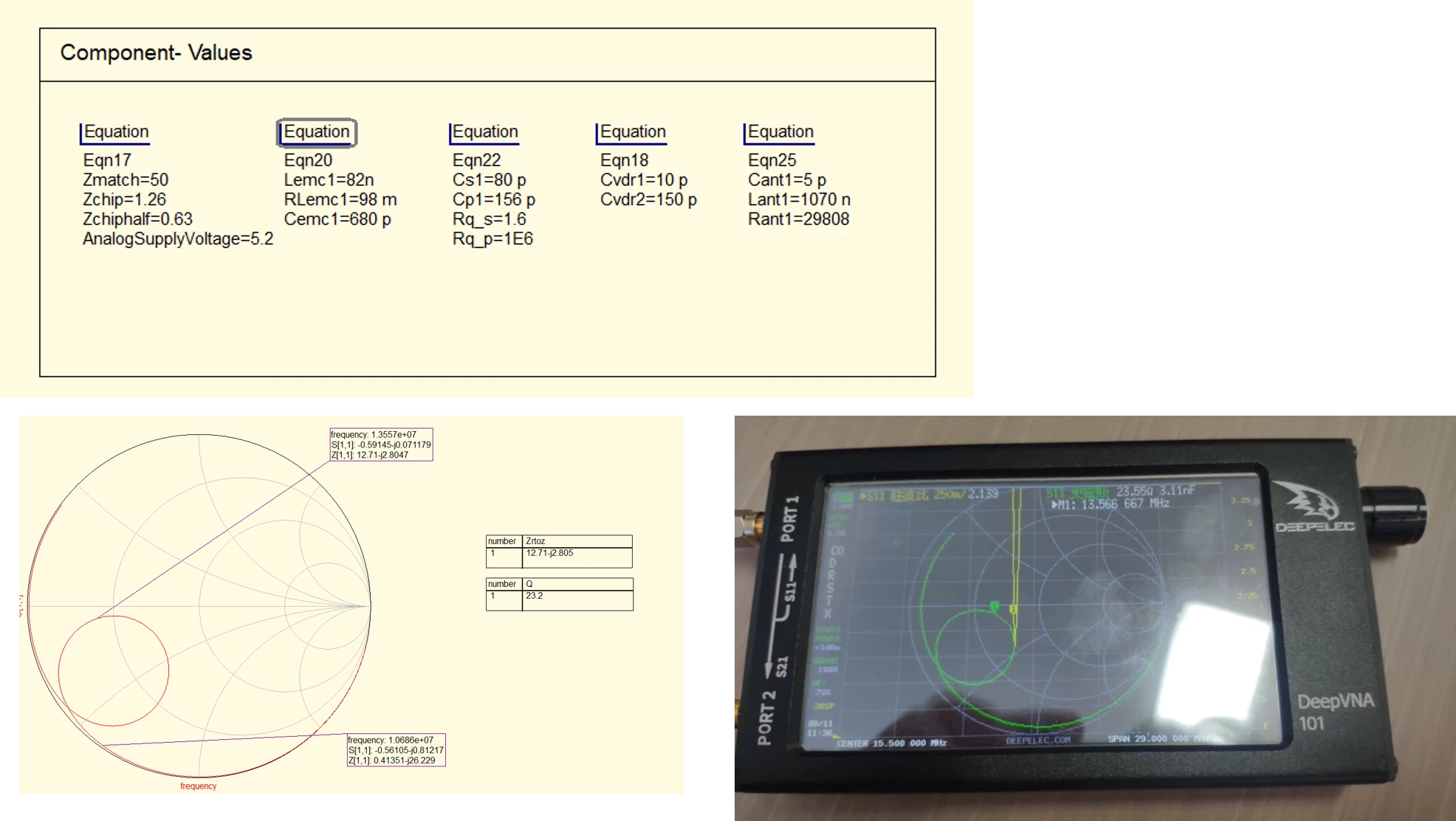
However, after actually building the circuit and measuring the antenna feed point with a NanoVNA, I obtained a significantly different result from the simulation.
The measured impedance was approximately:
Z ≈ 23.55 Ω − jX
The corresponding reactance is approximately equivalent to:
C ≈ 3.11 nF @ 13.56 MHz
My NanoVNA measurement setup is shown in Figure 3.
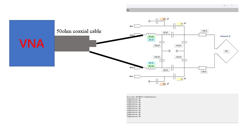
(This is the schematic diagram of the wiring I did during the test. On the actual PCB, it is not powered on. ST25R500 should default to the high-impedance state.)
This leads to my first question:
Why is there such a large difference between the impedance obtained from the official ST matching software simulation and the impedance measured in the actual hardware using the NanoVNA?
There is another issue that is even more confusing to me.
Based on the actual antenna impedance measured by the NanoVNA, I further adjusted the internal transmitter impedance setting of the ST25R500.
My initial understanding was that if the actual antenna/feed impedance was around 20 Ω, then setting the ST25R500 internal transmitter impedance to approximately 20 Ω should provide relatively good impedance matching.
I am using a 5 V supply, and I also applied the 1.75 factor specified in the datasheet when converting the internal impedance setting. Therefore, I set the internal impedance to approximately 20 Ω.
However, the actual test results showed a very counterintuitive phenomenon.
When the ST25R500 internal transmitter impedance was set to approximately 20 Ω, the reading distance was not optimal.
When I further reduced the internal impedance, and eventually set it to approximately:
2 Ω
the actual reading distance became significantly longer than when the impedance was supposedly matched.
This is very confusing to me.
According to the conventional understanding of impedance matching, the output impedance of the transmitter and the load impedance should be reasonably matched in order to achieve better power transfer. Therefore, I originally assumed that:
Transmitter output impedance ≈ Antenna/feed impedance
should result in a better reading distance.
However, my actual test results seem to show the opposite:
Internal impedance ≈ 20 Ω → shorter reading distance
Internal impedance ≈ 2 Ω → longer reading distance
Therefore, I would like to ask the following questions:
-
How should the target impedance in the official ST matching software be interpreted?
Is the target impedance the actual load impedance that should be presented to the ST25R500 RFO1/RFO2 outputs? -
Why is there such a significant difference between the simulation result from the official ST software and the impedance measured with the NanoVNA?
In this situation, should I use the simulated result as the reference, or should I primarily rely on the actual antenna/feed impedance measured at 13.56 MHz? -
What is the actual relationship between the ST25R500 internal transmitter impedance setting and the external antenna/load impedance?
Is it incorrect to simply assume that the best condition is achieved when the chip output impedance is equal to the antenna impedance? -
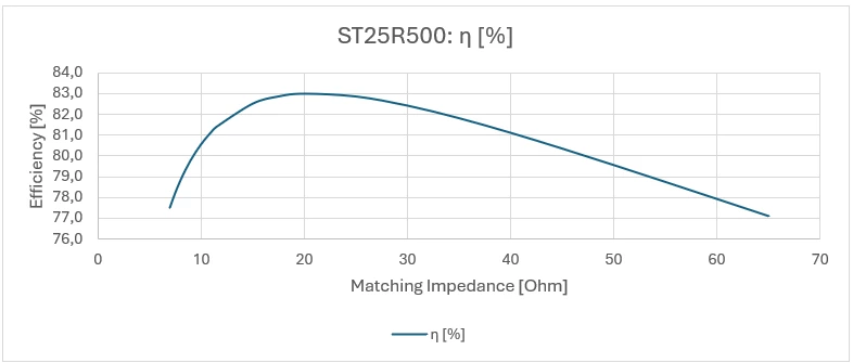
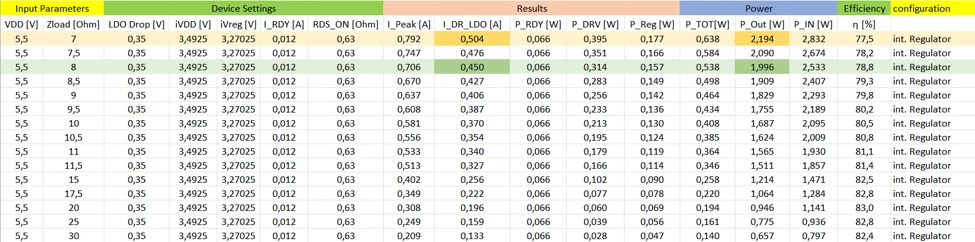
Why does reducing the ST25R500 internal impedance from approximately 20 Ω to approximately 2 Ω result in a longer reading distance?
Could this be related to the characteristics of the internal power amplifier/output stage, output current, load impedance, harmonics, matching network, or the actual voltage/current at the antenna? -
If my primary goal is to maximize the reading distance rather than minimize power consumption, which parameter should I focus on optimizing for the ST25R500?
Should I primarily optimize the transmitter output power, antenna current, antenna voltage, magnetic-field strength, or the power-transfer efficiency at the RFO output?
My actual measurements seem to indicate that simply achieving the best conventional impedance match does not necessarily result in the maximum reading distance.
Therefore, I suspect that there may be more involved here than conventional conjugate impedance matching, possibly related to the actual operating characteristics of the ST25R500 output stage.
If anyone has experience designing NFC/RFID readers using the ST25R500, ST25R3916, or other ST25R-series devices, I would greatly appreciate your help in analyzing this behavior.
In particular, I would like to understand the entire signal/power chain:
RFO output stage → matching network → antenna → actual antenna voltage/current → magnetic-field strength → tag coupling → reading distance
Any advice or technical explanation would be greatly appreciated.
Thank you very much!