
DIvan.1
Associate III
September 25, 2020
Solved

st25r3911B hardware deseign example

  • September 25, 2020
  • 4 replies
  • 1328 views

Hello!

I'm trying to develop my own PCB. Now I'm drawing an electrical scheme.

Now, I'm watching "X-CUBE NFC05A1" electrical scheme (LINK).

I have two questions:

1) Is there any other document how to draw electrical scheme for st25r3911B chip?

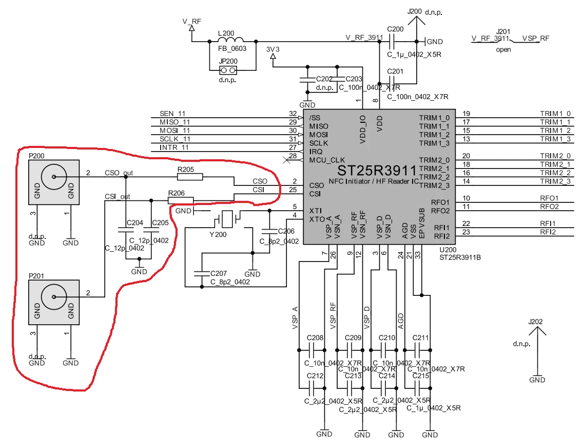
2) If I don't want to use "capacitive Wake-Up", do I need just to "skip" the red-crossed part on the picture below and leave pins CSO,CSI open or I need to use some other components?
0693W000004H7AwQAK.png

All the best,

Domen

This topic has been closed for replies.
Best answer by Travis Palmer

​Hello Domen,

Looks good.

You might can replace L1 by a 0R resistor. If you have too much filtering ( too much DC resistance in the supply) you might end up with ~4V at pin 8 (3911B VDD pin).

But this can be adjusted in the BOM.

When doing the layout you should take care that C28 and C32 are very close to the IC. I would recommend a similar layout as on the ST25R3911B-DISCO board.

Those caps are the driver decoupling capacitors and will have the most influence on switching noise due to the transmiter. They should have a solid connection to VSP_RF and VSN_RF.

Also C13 and C14 should be kept very close and on the same plane as the IC.

BR Travis

4 replies

Travis Palmer
ST Employee
September 28, 2020

Hello Domen,

If the capacitive sensing is not needed, all components can be left d.n.p. or even removed.

You can also use the electrical scheme of the ST25R3911B-DISCO but it shows a very similar schematic.

The UFL connector (P200, P201) have two purpose:

1.) Connect external capacitive patches

2.) Connect an oscilloscope to observe internal test (receiver) signals.

As you said, #1 is not required for your application.

For #2 I would recommend to place test points with very short traces close to the CSI and CSO pin.

If necessary you can connect wires or directly probe with a high impedance probe.

I would not recommend to add some long traces to the CSI / CSO pins.

br Travis

DIvan.1
DIvan.1Author
Associate III
September 29, 2020

Thank you for your informations Travis. It's very useful!.

I did it like It is in the picture below. Hope It's okey :)

0693W000004I2j5QAC.png

Best regards,

DomenI

Travis Palmer
Travis PalmerBest answer
ST Employee
September 29, 2020

​Hello Domen,

Looks good.

You might can replace L1 by a 0R resistor. If you have too much filtering ( too much DC resistance in the supply) you might end up with ~4V at pin 8 (3911B VDD pin).

But this can be adjusted in the BOM.

When doing the layout you should take care that C28 and C32 are very close to the IC. I would recommend a similar layout as on the ST25R3911B-DISCO board.

Those caps are the driver decoupling capacitors and will have the most influence on switching noise due to the transmiter. They should have a solid connection to VSP_RF and VSN_RF.

Also C13 and C14 should be kept very close and on the same plane as the IC.

BR Travis

DIvan.1
DIvan.1Author
Associate III
September 29, 2020

Thank you. You send the message just before I want to submit board to be made :)

I removed the L1, and move the condensators (C28, C32, C13, C14) even closer to the chip.

The picture below represent the PCB :)

0693W000004I5UwQAK.png

Best regarts,

DomenI