
DIvan.1
Associate III
Sep 25, 2020 10:29 AM UTC
Solved

st25r3911B hardware deseign example

Hello!

I'm trying to develop my own PCB. Now I'm drawing an electrical scheme.

Now, I'm watching "X-CUBE NFC05A1" electrical scheme (LINK).

I have two questions:

1) Is there any other document how to draw electrical scheme for st25r3911B chip?

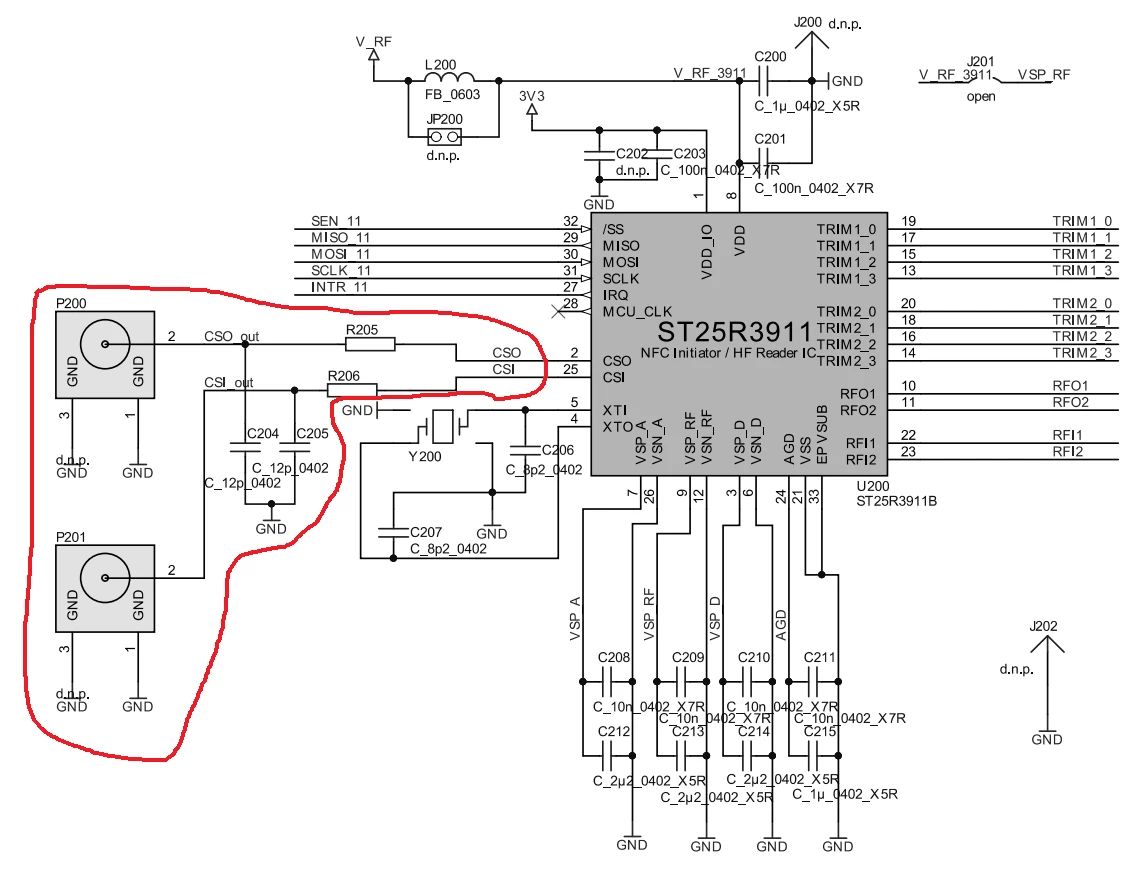
2) If I don't want to use "capacitive Wake-Up", do I need just to "skip" the red-crossed part on the picture below and leave pins CSO,CSI open or I need to use some other components?
0693W000004H7AwQAK.png

All the best,

Domen

This topic has been closed for replies.
Travis Palmer
Travis PalmerBest answer
ST Employee
Sep 29, 2020 7:14 AM UTC

​Hello Domen,

Looks good.

You might can replace L1 by a 0R resistor. If you have too much filtering ( too much DC resistance in the supply) you might end up with ~4V at pin 8 (3911B VDD pin).

But this can be adjusted in the BOM.

When doing the layout you should take care that C28 and C32 are very close to the IC. I would recommend a similar layout as on the ST25R3911B-DISCO board.

Those caps are the driver decoupling capacitors and will have the most influence on switching noise due to the transmiter. They should have a solid connection to VSP_RF and VSN_RF.

Also C13 and C14 should be kept very close and on the same plane as the IC.

BR Travis

4 replies

Travis Palmer
ST Employee
Sep 28, 2020 8:13 AM UTC

Hello Domen,

If the capacitive sensing is not needed, all components can be left d.n.p. or even removed.

You can also use the electrical scheme of the ST25R3911B-DISCO but it shows a very similar schematic.

The UFL connector (P200, P201) have two purpose:

1.) Connect external capacitive patches

2.) Connect an oscilloscope to observe internal test (receiver) signals.

As you said, #1 is not required for your application.

For #2 I would recommend to place test points with very short traces close to the CSI and CSO pin.

If necessary you can connect wires or directly probe with a high impedance probe.

I would not recommend to add some long traces to the CSI / CSO pins.

br Travis

DIvan.1
DIvan.1Author
Associate III
Sep 29, 2020 5:36 AM UTC

Thank you for your informations Travis. It's very useful!.

I did it like It is in the picture below. Hope It's okey :)

0693W000004I2j5QAC.png

Best regards,

DomenI

Travis Palmer
Travis PalmerBest answer
ST Employee
Sep 29, 2020 7:14 AM UTC

​Hello Domen,

Looks good.

You might can replace L1 by a 0R resistor. If you have too much filtering ( too much DC resistance in the supply) you might end up with ~4V at pin 8 (3911B VDD pin).

But this can be adjusted in the BOM.

When doing the layout you should take care that C28 and C32 are very close to the IC. I would recommend a similar layout as on the ST25R3911B-DISCO board.

Those caps are the driver decoupling capacitors and will have the most influence on switching noise due to the transmiter. They should have a solid connection to VSP_RF and VSN_RF.

Also C13 and C14 should be kept very close and on the same plane as the IC.

BR Travis

DIvan.1
DIvan.1Author
Associate III
Sep 29, 2020 10:22 AM UTC

Thank you. You send the message just before I want to submit board to be made :)

I removed the L1, and move the condensators (C28, C32, C13, C14) even closer to the chip.

The picture below represent the PCB :)

0693W000004I5UwQAK.png

Best regarts,

DomenI