

DMolo
Associate III
August 4, 2020
Question

Why does my Opamp PGA seem to be 10, not 16?

  • August 4, 2020
  • 16 replies
  • 3053 views

Hi,

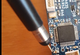
I have a board, with STM32f303. It generally works fine, but I am using the opamps and they are causing me trouble. I have set them up to have PGA of 16, and be internally connected to the ADC, and have test points on my board where I can measure the opamp output voltage. I can read the input voltage on the resistor-capacitor feeding it.

I observe that the opamp has almost exactly 100mV in (actually 102mV generated from a 4k7 pullup to 3v3 and 150ohm to ground, but only 1V out. It seems to be quite poorly defined on output, going between 0.8V and 1.35V. Obviously I expect 1.633V from 100mV*16 gain.

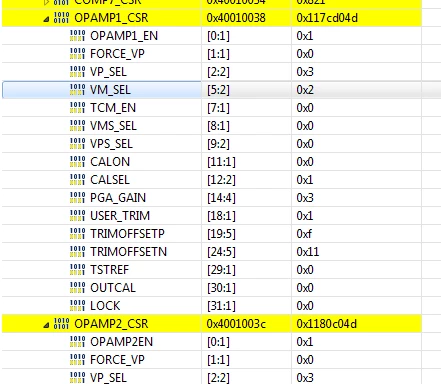
Registers are set as below, read out from the chip by the debugger while running; i.e. the actual values.

The opamp is actually being used to amplify the current on a 1mohm shunt. If I pass current through the shunt (driving a motor in open loop...), I can see the value change, but the opamp out is centred on ~1V

What is wrong? Is the chip just toasted?

I have tried setting calibration values, to no avail, manually setting TRIMOFFSETP and TRIMOFFSETN to the extreme values, but it doesn't get anywhere near central.

I also ran :

hopamp1.Init.Mode = OPAMP_STANDALONE_MODE ;
HAL_OPAMP_Init(&hopamp1);
HAL_OPAMP_SelfCalibrate(&hopamp1);
HAL_Delay(50);
 
hopamp1.Init.Mode = OPAMP_PGA_MODE;
HAL_OPAMP_Init(&hopamp1);

in the startup bit of main, and this generated different trim values, but still stayed near 1V.

My last resort will be to desolder and replace the chip... but I really can't think what I've done that could be nuking it. The analogue inputs are pretty gently loaded. The behaviour is the same on all 3 opamps I'm using, and given the rest of the chip works, I am disinclined to think static.
0693W000003C1qsQAC.png0693W000003C1qJQAS.png Thanks to everyone!

This topic has been closed for replies.

16 replies

waclawek.jan
Super User
August 4, 2020

> I observe that the opamp has almost exactly 100mV in (actually 102mV generated from a 4k7 pullup to 3v3 and 150ohm to ground, but only 1V out. It seems to be quite poorly defined on output, going between 0.8V and 1.35V. Obviously I expect 1.633V from 100mV*16 gain.

Which 'F303 is that, exactly? How do you measure the OPAMP output? How are the respective GPIO registers set? What is connected to it externally? Can you use a DC input, for testing, of different values than just the described one? What happens if you use a different gain setting?

JW

DMolo
DMoloAuthor
Associate III
August 4, 2020

f303CB

Measure it with oscilloscope, and/or DVM; both yeild the same results. Does the picture I uploaded not show?

Externally, the opamp is only connected to the test points, and there are several MOhm impedance on them when off - they're not shorted.

Different gain setting changes the value, but gain 8 results in actual gain of about 6, gain 4 actual gain about 3 etc.

So far I have tested with 0mV input (short input to ground) and got 0mV output on the opamp, and short to 3v3 and got 3v3 (saturated) on the output, and have forced a load of current through the shunt resistors, although not got values for that.

Doubling the pullup up with a second 4k7 resistor gives 200mV on input, and 2.5V on output (should be 3.2V)

I can potentially grab another power supply and stick other voltages on it... only got the one here at the moment though.

GPIOA registers as in the pics below:

0693W000003C2c3QAC.png

0693W000003C2fgQAC.png0693W000003C2fHQAS.png

DMolo
DMoloAuthor
Associate III
August 4, 2020

I've broken out the pins for opamp4, which was previously completely unused and untouched, and it has the same behaviour as the other 3. This leads me to believe I have not done something to damage the chip; it would be incredibly hard to have ESD'd or otherwise those pins; they were literally not broken out to anything atall.

So I went back to school, and sat with my multimeter, plotting input vs output on the broken out opamp4, and got the below:

0693W000003C5W3QAK.png

Dead straight small signal gain line of 16... but nowhere near through the origin. It seems this isn't really a rail to rail opamp, it's a kind of within 50mV of the rail opamp. The datasheet says CMIR 0-VDDA, and the input offset voltage is listed as 4mV maximum calibration range 6mV all conditions... nowhere near the 50mV I'm seeing.

I have another board running ST firmware from the MCWB, and that has a very small offset. I can't get my head around the code they've used to set it up... have they done some magic calibration, or is my chip just knackered?

Is this compensatable reliably, if, say I go and make thousands of these and don;t want to be trimming on a production line?

I guess I could go and start doing things like dynamically changing the gain setting to get the extra dynamic range, but I'd rather not have to.

waclawek.jan
Super User
August 4, 2020

50mV offset is disturbingly much indeed.

Is this offset seen if set as follower? Can anything of merit be measured on V- if configured to be brought out for "external filter"?

Can't this be done grounding-related issue? Is VSSA connected to VDD directly, aren't there soldering issues on this board? Isn't there any high current flowing into any ground pin? Could you check on another board, preferably a "known good" one such as Nucleo or Disco?

JW

DMolo
DMoloAuthor
Associate III
August 5, 2020

If I set it as follower, I put 100mV in and get 150mV out. umm :\

Unable to break out the V- due to the board design; those pins are connected to other lines that are a PITA to disconnect.

VDDA=VDD=3.287V supplied by a MIC5317 regulator. There are no detectable soldering flaws as measured with a multimeter coninuity (short pin:pin, short pin:ground, short pin:VCC, or pin disconnect). There is only this chip using the reg. The board, for the last experiment was powered from a USB, to free up my bench supply to do the injection, so there are definitely no large currents... Every VDD pin is decoupled with a ceramic 0603 cap (220nF) within 5mm of the pin. Every ground pin is coupled to the ground plane within 5mm of the pin by a via. The ground plane is pretty solid. Very solid. It's not the problem; in fact, I am amazed at how clean my current trace measurements are despite being offset by the ~700mV.

I'll see about trying with a nucleo or Disco later, I'm coming round to the prospect of getting out the hot air station and replacing the chip, I feel like that might be less work that porting the code to a nucleo and wiring that up.

waclawek.jan
Super User
August 6, 2020

More humm.

You've double-checked also the analog supply/ground pins.

Analog supply is tightly within digital. (I see above this is check)

There is no injection through the protection diodes, i.e. input (including digital on TT pins) forced above lowest supply or below ground.

There is no ground bond overload, i.e. no output fighting against hard opposite level from outside.

Hot air is one of the options, too, but I personally would triple check for errors in the circuitry first. Two permanently damaged chips are more annoying than one permanently damaged chip.

JW

DMolo
DMoloAuthor
Associate III
August 6, 2020
I have some 5V sensors inputting onto port b pins through 4k7 resistors, but they are all on five tolerant FT pins​... I haven't misinterpreted five tolerant have I? In any case the fault persists when they're unplugged.

Solder station is a 20 minute job once i take a breath and commit. ​the price of the chip is... Frankly irrelevant compared to the time I'm losing.

Actually, since I have spare unpopulated pcbs, the easiest option might be to solder the bare minimum components to that to do the test.​

I don't think there's any pin fighting as you describe. The fault persists even with all other pins and peripherals in reset state.​
waclawek.jan
Super User
August 11, 2020

Your findings are not very comforting... but thanks for sharing them.

JW

DMolo
DMoloAuthor
Associate III
August 17, 2020

Update to this: I have now tried with 4 different STM32f303CB chips, on 3 different boards. They all fall short on the output voltage. Some by more than others, but all well short (minimum 70mV short, one was 150mV short).

I guess the first one with 600mV offset might have been damaged, the other 3 definitely were not.

Currently I have one programmed with the ST FOC setup, and it runs OK, but the "All FETs disabled" output is 1.55V, when it should be 1.63.

As long as it's stable, I can shrug and say "Meh", less than 100mV can just be subtracted out for this application, but it's a bit disappointing really, and strongly limits the applicability to applications where it's possible to do compensation.

David

waclawek.jan
Super User
August 18, 2020

Hi David,

Thanks for coming back with the results.

You might want to contact ST through the web support form or through FAE. They probably would like to have you to produce a minimum program reproducing the problem on a Nucleo/Disco. I'd really like to hear their explanation.

JW

waclawek.jan
Super User
August 18, 2020

I have a 'F303RBT6 (datecode 905) in one setup. Tried to set OPAMP4 to follower OPAMP4->CSR=0x1070006d and measured voltage between OPAMP4's VP and output (PB10 and PB12). That changed from 0mV to cca 4mV while VP changed from 0mV to 2V. Then I set it to gain 2 and took the following measurements:

VP Vout

1,000V 1,9807V

0,5004V 0,9876V

0,2022V 0,3952V

From this the input offset appears to be around 3.5mV.

Not perfect, but viable (in our application, there will be an independent calibration - we are using combination of internal and external feedback, user-configurably; and the purpose of our application requires calibration after reconfiguration anyway).

I'll try to keep an eye on the issue, maybe adding a check of the offset to the production test procedure. I admit your findings do scare me a bit.

JW
