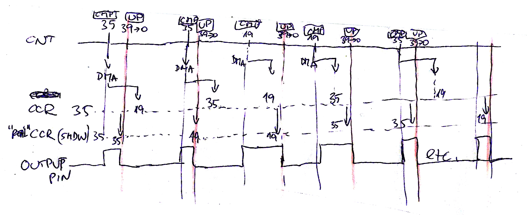
DMA PWM outputs 2 pulses per buffer value (STM32l072xx)
I'm trying to use DMA in circular mode to modify the duty cycle of a PWM output. Ultimately, I plan to use it to communicate with WS2812B chips (like others have done with the STM32F4 chips). However, in my early tests I've noticed that it seems to send two pulses per buffer value.
For a simple example (full code at the end):
#define BUFFER_SIZE 2

uint16_t buffer[BUFFER_SIZE];
buffer[0] = htim3.Init.Period * .5; // 50%
buffer[1] = htim3.Init.Period * .9; // 90%

HAL_TIM_PWM_Start_DMA(&htim3, TIM_CHANNEL_1, (uint32_t*)buffer, BUFFER_SIZE);
There are 2 items in the buffer, one set at 50% duty cycle and the other at 90%. When circular mode is enabled, I would expect to see the PWM pulse to be alternating between the two. However, I see 2 pulses at 50% followed by 2 at 90%, and so on.
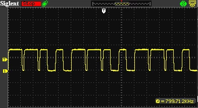
I'm sure I'm missing something elementary here. How do I get the pulses to alternate 50%, 90%, 50%, etc?
One of my thoughts was that the duplication could be caused by data width conversion on the data bus, as explained in section 11.3.4, page 268, of the reference manual (i.e. 16-bit value on a 32-bit bus) However, changing the DMA Data Alignment values doesn't change this.
Any ideas? Here's the code, which is based on the boiler plate created by STM32Cube:
#include <stdint.h>
#include "main.h"

#define SIGNAL_HZ 800000 // 800kHz
#define BUFFER_SIZE 2

TIM_HandleTypeDef htim3;
DMA_HandleTypeDef hdma_tim3_ch1;
uint16_t buffer[BUFFER_SIZE];

void SystemClock_Config(void);
static void MX_GPIO_Init(void);
static void MX_TIM3_Init(void);
static void MX_DMA_Init(void);

/**
 * @brief The application entry point.
 * @retval int
 */
int main(void) {
 HAL_Init();
 SystemClock_Config();
 MX_GPIO_Init();
 MX_DMA_Init();
 MX_TIM3_Init();

 // PWM Buffer
 buffer[0] = htim3.Init.Period * .5; // 50%
 buffer[1] = htim3.Init.Period * .9; // 90%

 // Start DMA -> PWM
 HAL_TIM_PWM_Start_DMA(&htim3, TIM_CHANNEL_1, (uint32_t*)buffer, BUFFER_SIZE);

 while (1) { }
}

/**
 * @brief System Clock Configuration
 * @retval None
 */
void SystemClock_Config(void)
{
 RCC_OscInitTypeDef RCC_OscInitStruct = {0};
 RCC_ClkInitTypeDef RCC_ClkInitStruct = {0};

 __HAL_PWR_VOLTAGESCALING_CONFIG(PWR_REGULATOR_VOLTAGE_SCALE1);

 // Oscillator init config
 RCC_OscInitStruct.OscillatorType = RCC_OSCILLATORTYPE_HSI;
 RCC_OscInitStruct.HSIState = RCC_HSI_ON;
 RCC_OscInitStruct.HSICalibrationValue = RCC_HSICALIBRATION_DEFAULT;
 RCC_OscInitStruct.PLL.PLLState = RCC_PLL_ON;
 RCC_OscInitStruct.PLL.PLLSource = RCC_PLLSOURCE_HSI;
 RCC_OscInitStruct.PLL.PLLMUL = RCC_PLLMUL_4;
 RCC_OscInitStruct.PLL.PLLDIV = RCC_PLLDIV_2;
 if (HAL_RCC_OscConfig(&RCC_OscInitStruct) != HAL_OK) {
 Error_Handler();
 }

 // Clock init config
 RCC_ClkInitStruct.ClockType = RCC_CLOCKTYPE_HCLK|RCC_CLOCKTYPE_SYSCLK
 |RCC_CLOCKTYPE_PCLK1|RCC_CLOCKTYPE_PCLK2;
 RCC_ClkInitStruct.SYSCLKSource = RCC_SYSCLKSOURCE_PLLCLK;
 RCC_ClkInitStruct.AHBCLKDivider = RCC_SYSCLK_DIV1;
 RCC_ClkInitStruct.APB1CLKDivider = RCC_HCLK_DIV1;
 RCC_ClkInitStruct.APB2CLKDivider = RCC_HCLK_DIV1;
 if (HAL_RCC_ClockConfig(&RCC_ClkInitStruct, FLASH_LATENCY_1) != HAL_OK) {
 Error_Handler();
 }
}

/**
 * @brief TIM3 Initialization Function
 * @param None
 * @retval None
 */
static void MX_TIM3_Init(void) {
 TIM_MasterConfigTypeDef sMasterConfig = {0};
 TIM_OC_InitTypeDef sConfigOC = {0};

 __HAL_RCC_TIM3_CLK_ENABLE();

 htim3.Instance = TIM3;
 htim3.Init.Prescaler = 0;
 htim3.Init.CounterMode = TIM_COUNTERMODE_UP;
 htim3.Init.Period = (SystemCoreClock / SIGNAL_HZ) - 1;
 htim3.Init.ClockDivision = TIM_CLOCKDIVISION_DIV1;
 htim3.Init.AutoReloadPreload = TIM_AUTORELOAD_PRELOAD_ENABLE;
 if (HAL_TIM_PWM_Init(&htim3) != HAL_OK) {
 Error_Handler();
 }

 sMasterConfig.MasterOutputTrigger = TIM_TRGO_RESET;
 sMasterConfig.MasterSlaveMode = TIM_MASTERSLAVEMODE_DISABLE;
 if (HAL_TIMEx_MasterConfigSynchronization(&htim3, &sMasterConfig) != HAL_OK) {
 Error_Handler();
 }

 sConfigOC.OCMode = TIM_OCMODE_PWM1;
 sConfigOC.Pulse = 0;
 sConfigOC.OCPolarity = TIM_OCPOLARITY_HIGH;
 sConfigOC.OCFastMode = TIM_OCFAST_ENABLE;
 if (HAL_TIM_PWM_ConfigChannel(&htim3, &sConfigOC, TIM_CHANNEL_1) != HAL_OK) {
 Error_Handler();
 }
 if (HAL_TIMEx_RemapConfig(&htim3, TIM3_TI1_GPIO) != HAL_OK) {
 Error_Handler();
 }
}

/**
 * Enable DMA controller clock
 */
static void MX_DMA_Init(void){
 __HAL_RCC_DMA1_CLK_ENABLE();

 hdma_tim3_ch1.Instance = DMA1_Channel5;
 hdma_tim3_ch1.Init.Request = DMA_REQUEST_10;
 hdma_tim3_ch1.Init.Direction = DMA_MEMORY_TO_PERIPH;
 hdma_tim3_ch1.Init.PeriphInc = DMA_PINC_DISABLE;
 hdma_tim3_ch1.Init.MemInc = DMA_MINC_ENABLE;
 hdma_tim3_ch1.Init.PeriphDataAlignment = DMA_PDATAALIGN_WORD; // 16-bit PWM, but 32-bit bus
 hdma_tim3_ch1.Init.MemDataAlignment = DMA_MDATAALIGN_HALFWORD;
 hdma_tim3_ch1.Init.Mode = DMA_CIRCULAR;
 hdma_tim3_ch1.Init.Priority = DMA_PRIORITY_LOW;
 if (HAL_DMA_Init(&hdma_tim3_ch1) != HAL_OK) {
 Error_Handler();
 }
 __HAL_LINKDMA(&htim3, hdma[TIM_DMA_ID_CC1], hdma_tim3_ch1);
}

/**
 * @brief GPIO Initialization Function
 * @param None
 * @retval None
 */
static void MX_GPIO_Init(void) {
 GPIO_InitTypeDef GPIO_PWMStruct = {0};
 __HAL_RCC_GPIOA_CLK_ENABLE();

 // PWM output pin - PA6
 GPIO_PWMStruct.Pin = GPIO_PIN_6;
 GPIO_PWMStruct.Mode = GPIO_MODE_AF_PP;
 GPIO_PWMStruct.Pull = GPIO_PULLDOWN;
 GPIO_PWMStruct.Speed = GPIO_SPEED_FREQ_VERY_HIGH;
 GPIO_PWMStruct.Alternate = GPIO_AF2_TIM3;
 HAL_GPIO_Init(GPIOA, &GPIO_PWMStruct);
}

/**
 * @brief This function is executed in case of error occurrence.
 * @retval None
 */
void Error_Handler(void) {
}