ravix475
Associate II
July 23, 2015
Question

Trouble communicating with a new board design - SWD ERROR

  • July 23, 2015
  • 5 replies
  • 1134 views
Posted on July 24, 2015 at 01:19

This is my first project with an STM part. I have started development on a NUCLEO board with an STM32F401RE chip and I'm programming/debugging using the onboard STLINKv2. So far firmware development has gone well. 

I designed a new board with the same chip (STM32F401RE) and I bought a second NUCLEO board to harvest the STLINK from. 

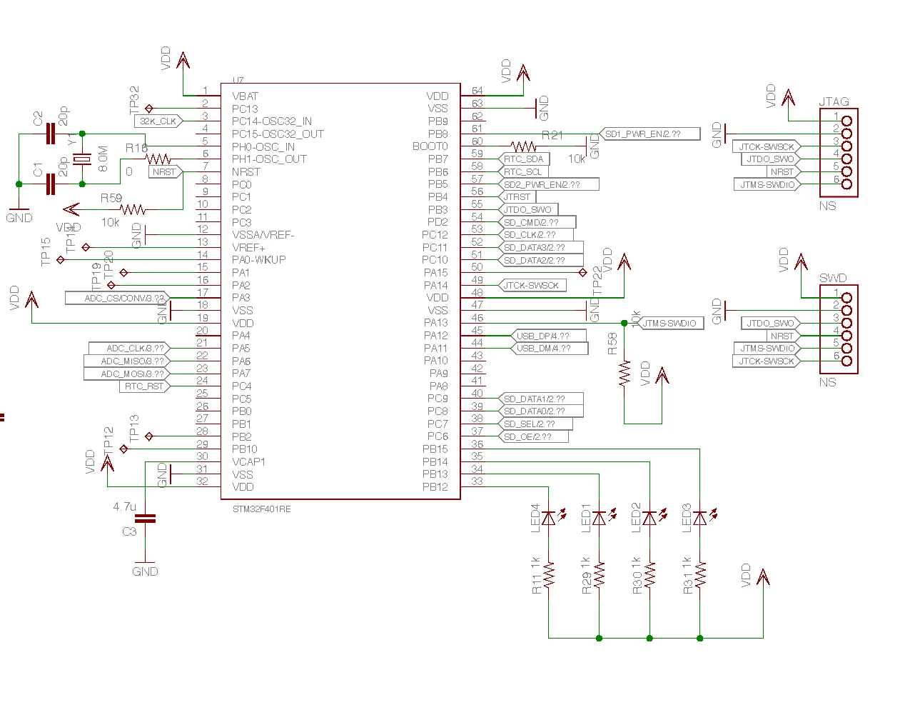
I cannot communicate with the new pcb at all -- from either STLINK, and I'm afraid I might have done something wrong in my schematic. 

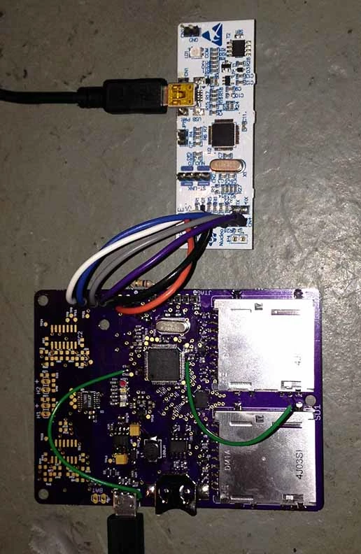
I am attaching the schematic and a picture of my programming setup. 

Some notes: 

1. I have removed the CN4 jumpers on the STLINK board

2. I have tried with only SWDIO, SCK, GND, and VDD  (also trying with SWO and NRST)

3. I have tried various configurations of BOOT0, BOOT1, although by default BOOT0 = GND. 

4. I have tested continuity all the way between the pins and the STLINK and made the wires shorter. 

No matter what I do, when I plug in the STLINK board, the NUCLEO drive contains a file called fail.txt, which contains the text ''SWD ERROR''. And I am unable to connect or communicate with the target board from the STLINK software. 

0690X00000605F7QAI.png0690X000006033HQAQ.jpg

    This topic has been closed for replies.

    5 replies

    Tesla DeLorean
    Guru
    July 24, 2015
    Posted on July 24, 2015 at 02:19

    Can you attach a better focused/resolution picture, rather than in-line (100kb) one?

    Check the voltage on the VCAP pin, and the NRST pin.

    Can you use the ST-LINK Utilities rather than the on-board mass-storage method?

    The board looks to have it's own supply, if so *don't* connect VDD to the ST-LINK

    Tips, Buy me a coffee, or three.. PayPal Venmo (See Profile) Up vote any posts that you find helpful, it shows what's working..
    raptorhal2
    Lead
    July 24, 2015
    Posted on July 24, 2015 at 15:54

    The functional connections to the SWD are incorrect. E.g., GND is pin 3. Check Section 5.2.4 in the Nucleo reference manual.

    Cheers, Hal

    ravix475
    ravix475Author
    Associate II
    July 24, 2015
    Posted on July 24, 2015 at 19:45

    Thank you for putting me on the right track. I checked VCAP1 and saw that the 1.2V rail was failing to come up properly. I tried replacing the capacitor on VCAP1 with the one from my spare NUCLEO board without any change. After reviewing the reference manual I found that VDD - VREF+ cannot be greater than 1.2V. I had VREF+ unconnected. 

    After connecting VREF+ to VDD the chip powered up successfully. 

    V

    DDA

    V

    REF+

    < 1.2 V 

    ravix475
    ravix475Author
    Associate II
    July 24, 2015
    Posted on July 24, 2015 at 19:46

    Hi Hal, 

    Thanks for the review. You are, of course, correct. But I am already re-arranging the wires in between the boards to correct this. 

    Tesla DeLorean
    Guru
    July 24, 2015
    Posted on July 24, 2015 at 19:51

    After connecting VREF+ to VDD the chip powered up successfully

    I was looking for VDDA on your design, assuming that's the VREF+. The Power-On-Reset circuit and PLL are run off the analogue supply. The parts won't start without it.

    Pin 13 on the 64-pin devices is VDDA, +VREF is connected to it internally.
    Tips, Buy me a coffee, or three.. PayPal Venmo (See Profile) Up vote any posts that you find helpful, it shows what's working..