
Solved
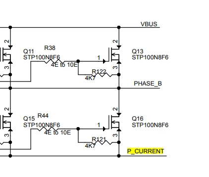
What is the P_CURRENT in STDES-EVT001V1 design, please help me out to know what exactly it is ?

Very well spotted!
However, this is the 2nd capacitor bank (C21-22, C25..28, C30-31) with a total capacity of 1320µF directly buffering spike currents. They are therefore directly connected between the drain of the high-side FET and the source of the low-side FET.
The main capacitor bank (C17-20, C23-C24) between VBUS and GND provides a total capacity of 2820µF.
The single-shunt is located between the negative pole of the main capacitor bank and the negative pole of the 2nd capacitor bank you mentioned, which can also be seen in the layout using a GERBER viewer.
Regards
/Peter
Enter your E-mail address. We'll send you an e-mail with instructions to reset your password.
