Your layout needs some improvement: please keep in mind that this is a inductive switching regulator, the layout of which must be carefully planned. E.g. route the feedback trace as far away as possible from power inductors and other noisy power traces, and keep it as short and with low-inductance and with low-resistance as possible.
You can take e.g. a look at the layout of the very similar STEVAL-VP319X1B, especially the application note AN5521. There you will also find the layout as GERBER ZIP file, which you are welcome to adopt and adapt whatever you like.
If you don't have a GERBER viewer, you can use the tool GerbView, for example, which is part of the KiCad program package and is also able to open GERBER ZIP files directly.
Good luck!
If the problem is resolved, please mark this topic as answered by selecting Select as best. This will help other users find that answer faster.
/Peter
In order to give better visibility on the answered topics, please click on Accept as Solution on the reply which solved your issue or answered your question.



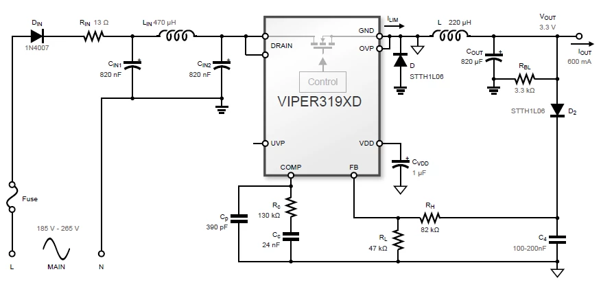
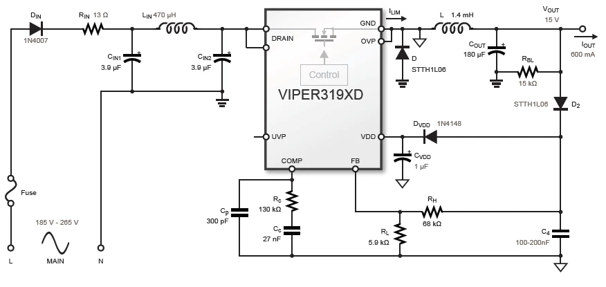 I made two boards according to these diagrams:
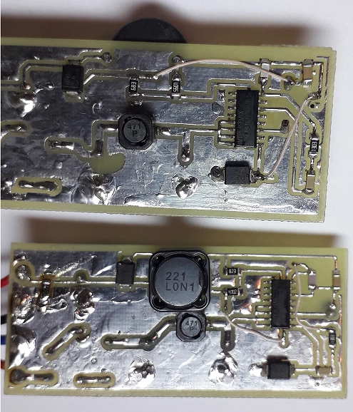
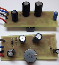 In the process of testing them, I found that in the absence of a load, the voltage at the output of the circuits is 3.8 and 16 volts. Then I set a current of 100 mA from the electronic load and the voltage dropped to almost zero. Maybe the board went to the defense?