

PWD13F60 Interference between MOSFET pairs in full-bridge frequency converter
Hello to everyone. I'm making a 200W frequency converter for motor driving with APFC (~85...265 AC input) at my own 2-layers PCB and have some questions about influence from one half-bridge to another half-bridge inside the IC.
Parts are driven in unipolar modulation mode: HIN1, LIN1 are driven with 23.1 kHz square-wave signals (dead-time 1 us) which represent sine wave signal as their duty cycle is proportional to sinus amplitude (lets call it HF part). HIN2, LIN2 are driven with 10...100 Hz simple square-wave (lets call it LF part), the load is connected to OUT1-OUT2 with filter (3 mH, 3 uF) and the output is sine-wave signal with frequency of LF signal. 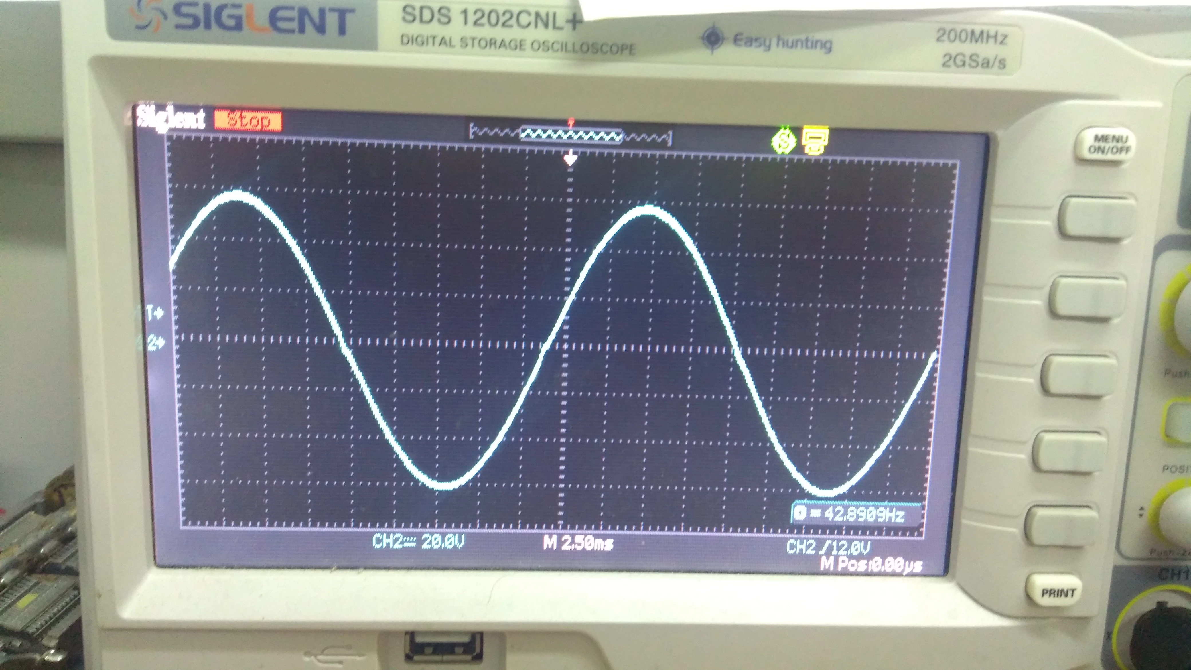
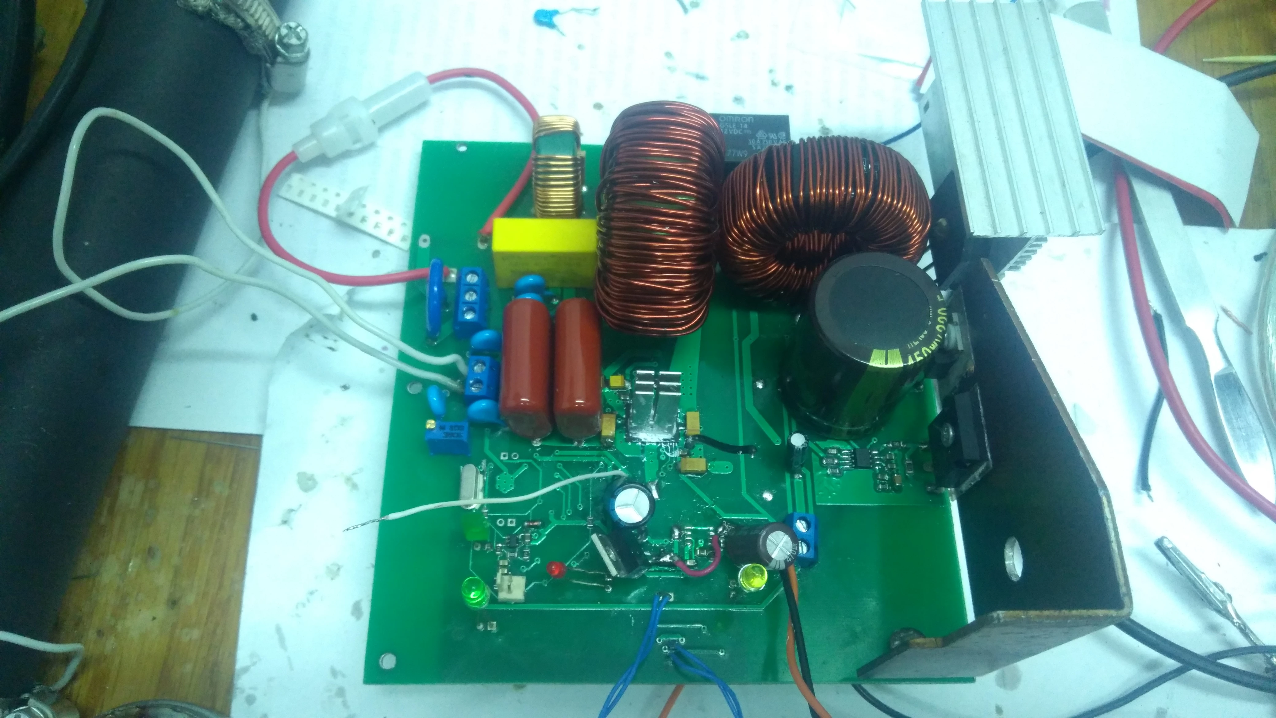
VS=60V, impulse amplitude at inputs of PWD13F60 is 5V, VCC=15V, the PCB is shown below (APFC is at the right and is in OFF state, VS was taken from lab power supply).
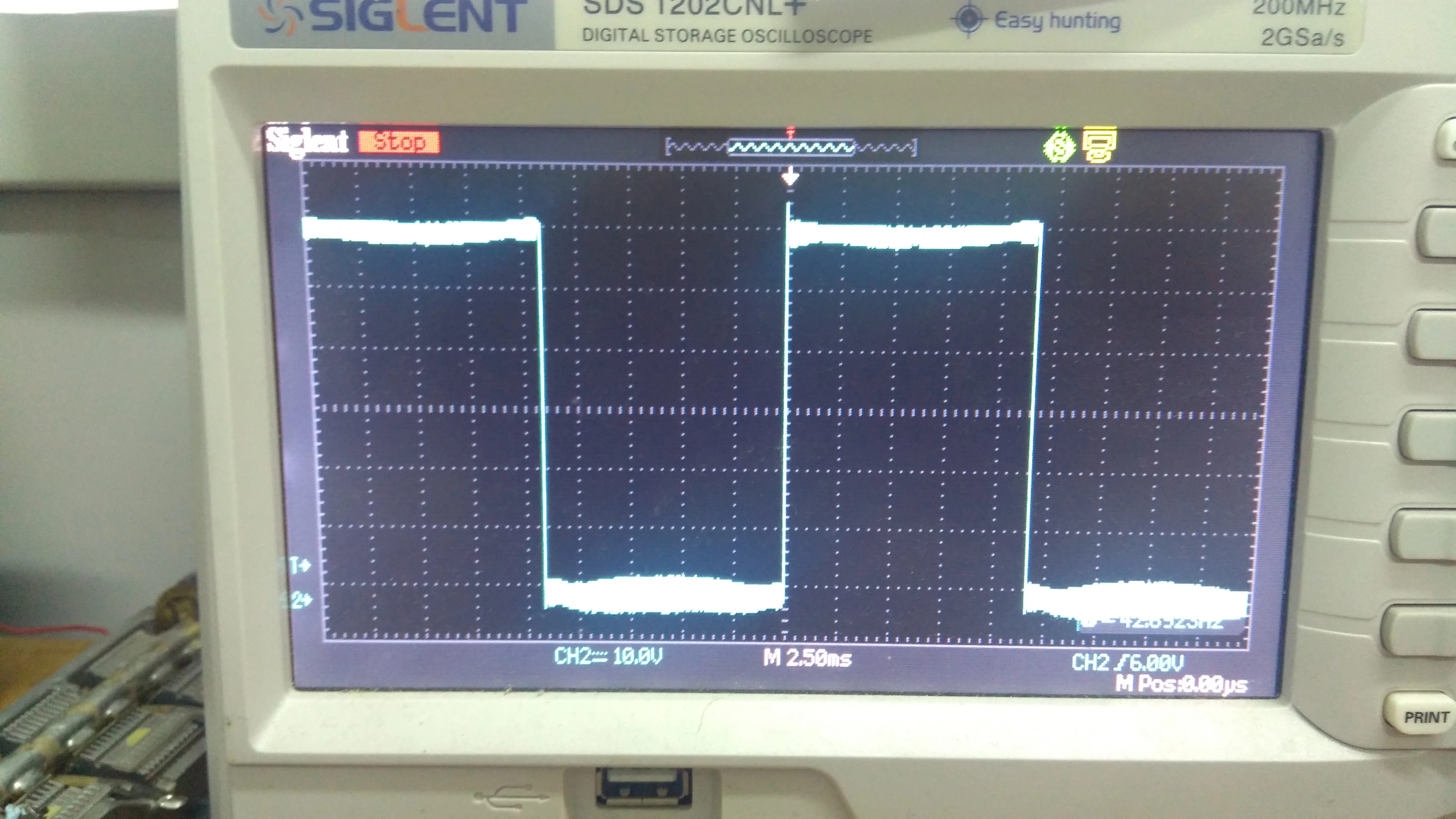
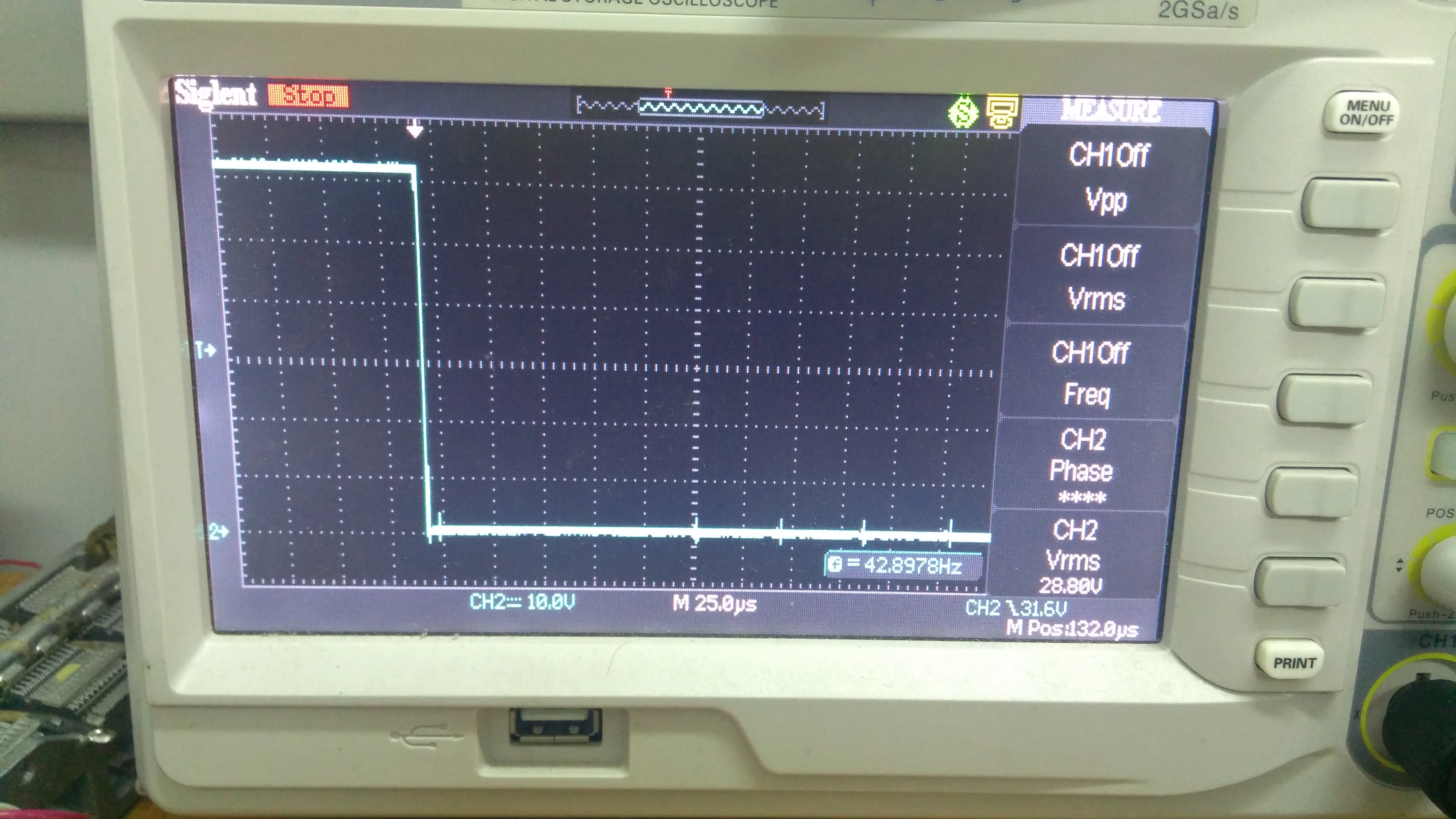
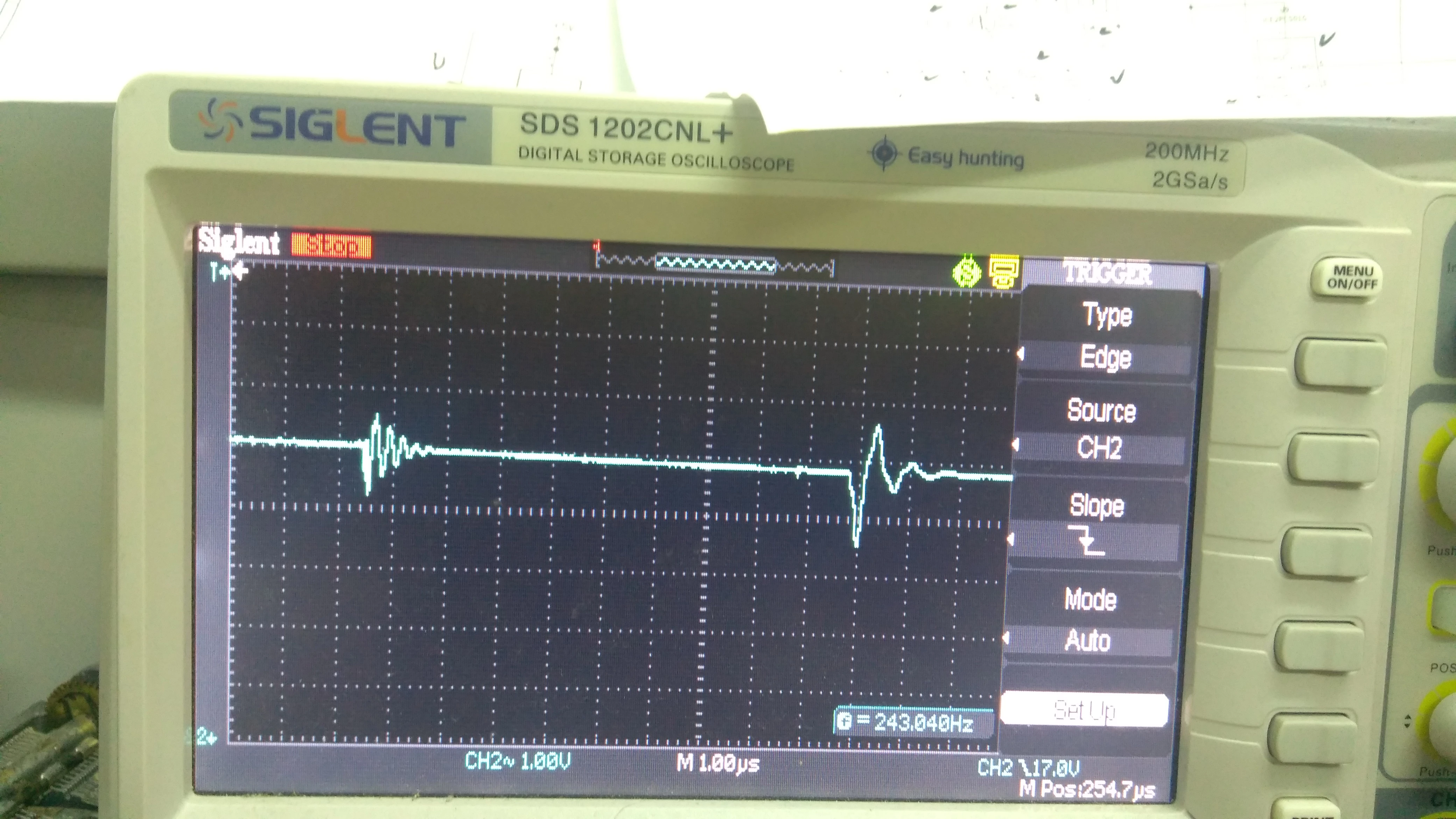
While measuring there is repeating interference at LF impulse with frequency of HF switching and its amplitude is dependent from VS, so at some VS value this interference become so huge that it opens LF part FET while it needs to be closed (!!!) and I have overcurrent protection enabling.
zoomed:
impulses:
And waveform of HF signals are suitable as for "upper FET" and for "lower FET" as can be seen:
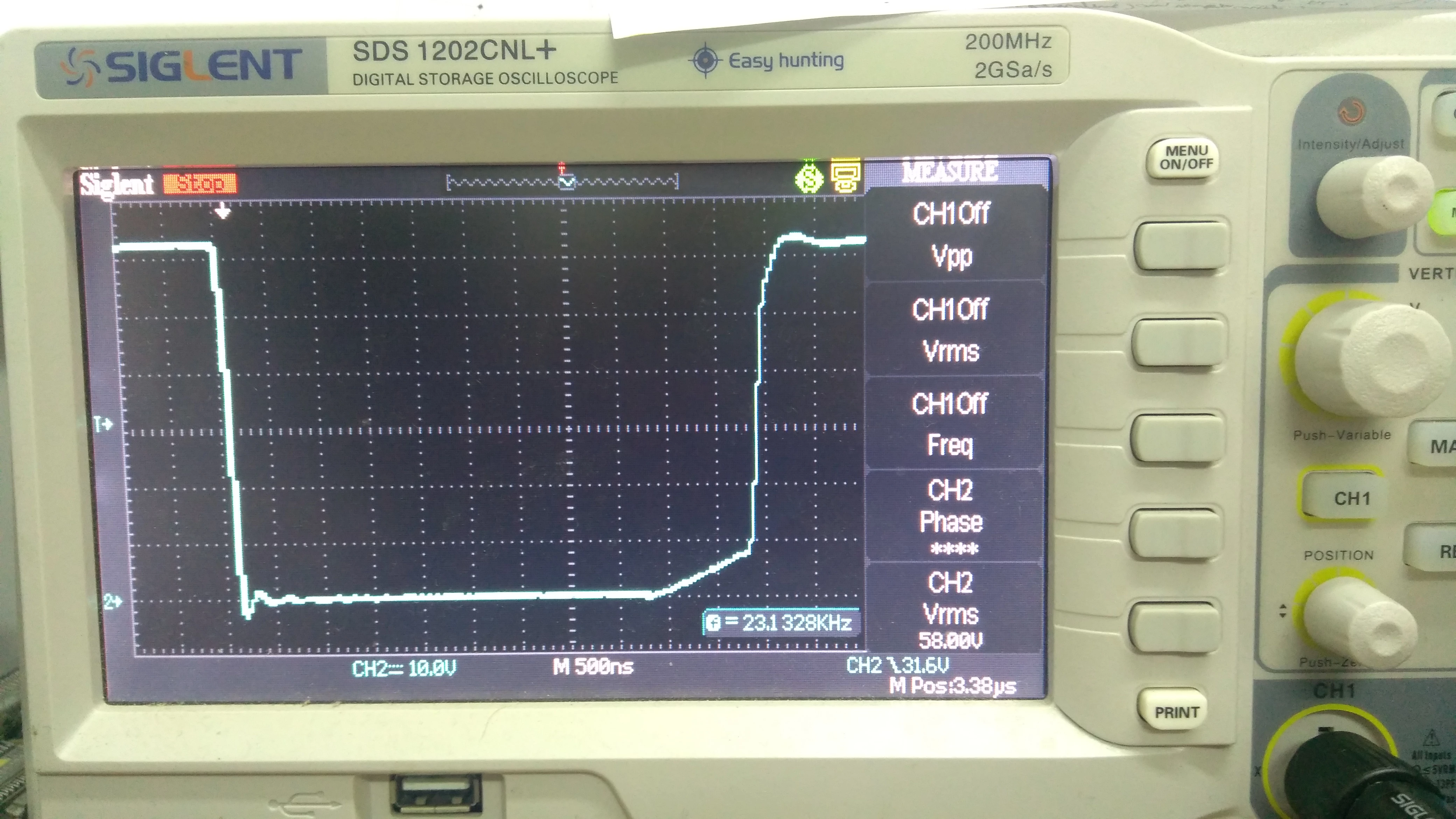
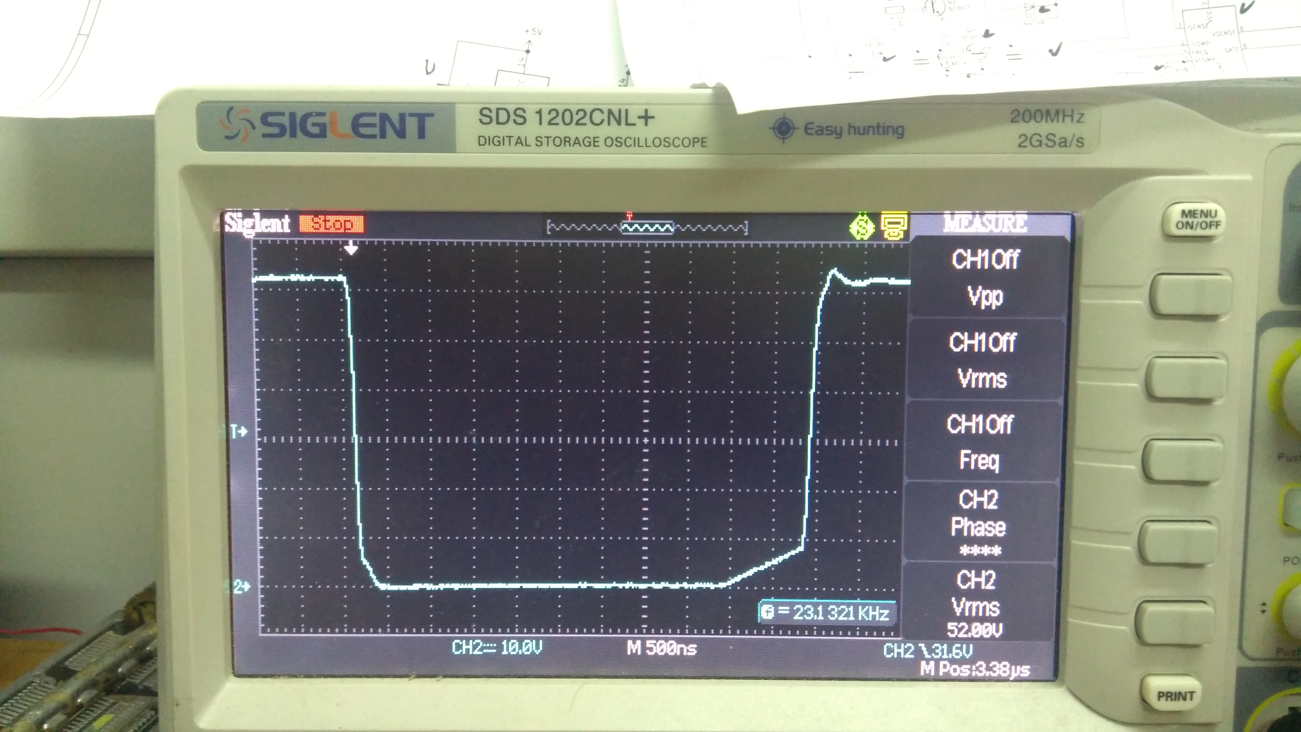
My question is:
Can it be because of inner intercoupling capacitance of IC or I need to modify my PCB and maybe add LPF to LF inputs of PWD13F60 IC? Do I need to use maybe full GND polygon under IC or there is some addition hints.
I have read about distances of 1.2mm between VS and other pads and will remake layout (was 1,05.....1,15mm) so is it need to remake something else. Or the whole PCB?:)
Thank you in advance!
P.S. The case temperature was about 60 C under 0.9A load and 60V VS and also dependent from VS value (VS=30V, 0.9A and only 45 deg temperature). Charge dissipation increase???
