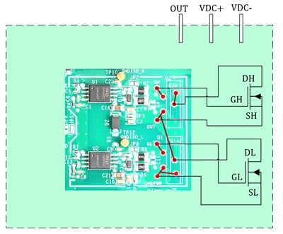
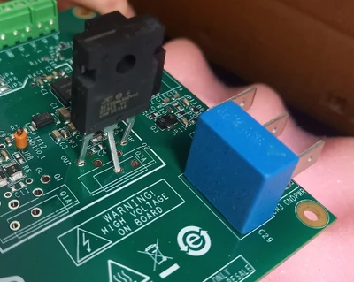
Actually, the double white line at the marking for Q1 and Q2 should indicate that the tab side of the transistor must face this side. Your MOSFET is therefore inserted the wrong way round: in your photo, the pin sequence of the MOSFET is gate-drain-source from the left, but it should be source-gate-drain, as shown correctly in your schematic.
In this context, the question also arises as to whether the SCTxxx visible in the photo, i.e. a SiC-MOSFET should be used for your test?
Are you aware that STGAP2HS is intended for IGBT and Si-MOSFET only and that STGAP2SICS or STGAP2SICSN should be used for SiC-MOSFET?
The outer solder connections, which deviate from the triangular arrangement of the transistor holes, are intended for the unpopulated C28 (27.5mm), but this is marked on the underside of the board.
Hope that helps?
Regards
/Peter
In order to give better visibility on the answered topics, please click on Accept as Solution on the reply which solved your issue or answered your question.