

EVAL6498L gate driving board
Hi there,
I am using EVAL6498L to test a boost converter having one switch and one diode.
I was wondering if I can use a synchronous rectifier in my boost converter, in other words if it is possible to control both switches (one high side switch and one low side switch), using EVAL6498L.
From the schematic I have found in the datasheet of 6498L gate driver, it seems that the 6498L IC is made on-purpose to control a high-side and a low-side switch in the same switching leg.
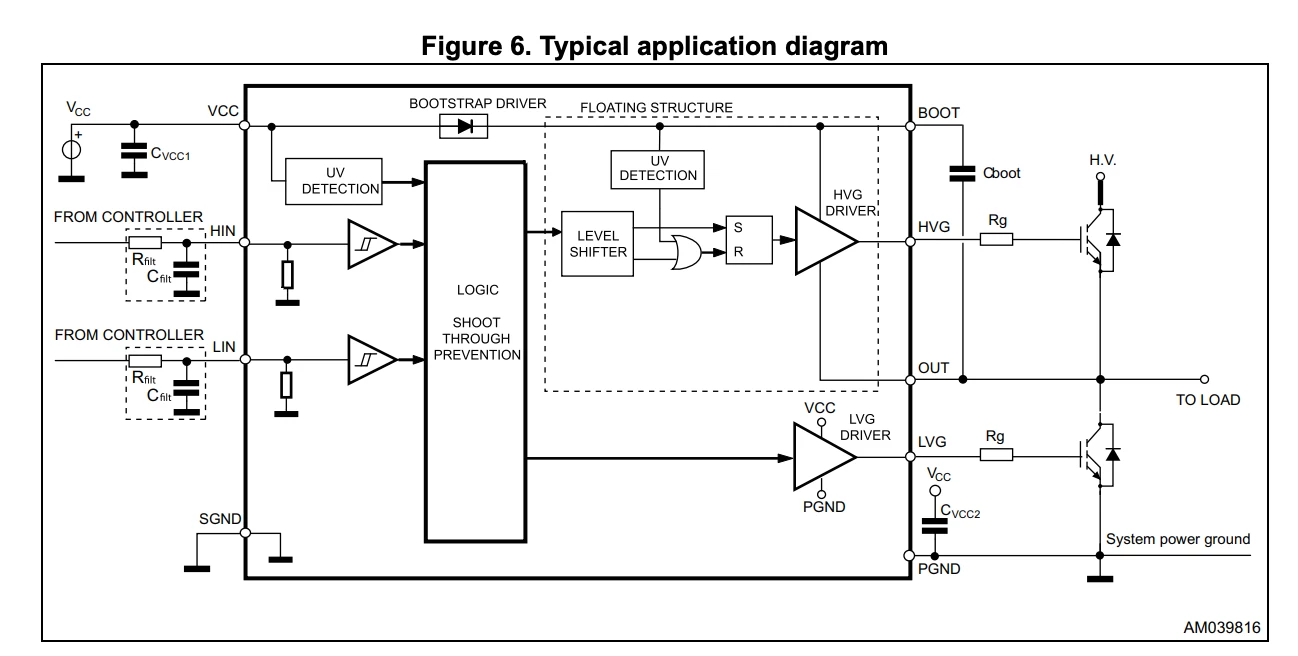
However, what I am not sure about is the connections on the "From Controller" on the left side of the drawing. In particular,
1) if I provide a PWM from a microcontroller which has one ground reference, connected to SGND, do I need to galvanically isolate the top PWM going to the gate driver? (i.e. does the PWM signal going to HIN need to be galvanically isolated? - that is not referenced to SGND)
2) I am a bit confused about SGND and PGND, I understand that these are signal and power ground, where the signal ground is connected to the microcontroller ground. The power ground is the converter ground. What I would like to clarify is that if these two grounds are connected inside the gate driver? and if not, is the connection of SGND and PGND recommended at all?
Thank you very much
Lello
