


yigitdurak
Explorer II
Jul 8, 2026 11:51 PM UTC
Solved

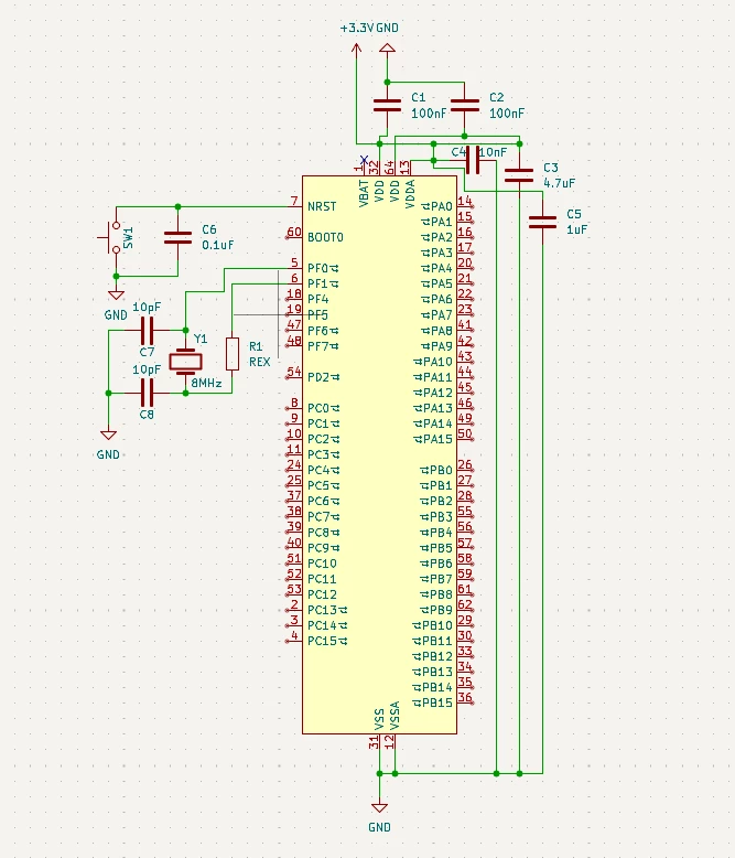
Request for review of power connection schematic for stm32f051r8t6

Dear team, hello, I've drawn a power supply circuit diagram for the STM32F051R8T6 but I'm a little hesitant. The diagram of my circuit is below. Have I done it correctly? Thank you for your answer.

 

TDK
TDKBest answer
Jul 9, 2026 1:18 AM UTC

BOOT0 should be tied or pulled to ground.

You need some way to program it. An SWD connection on a standard programming header like STLINK-V3MINIE or similar is recommended.

Otherwise, looks good.

Power nets and decoupling capacitors could be drawn a bit cleaner.


Follow the design guide:

https://www.st.com/resource/en/application_note/an4080-getting-started-with-stm32f0x1x2x8-hardware-development-stmicroelectronics.pdf

"If you feel a post has answered your question, please click ""Accept as Solution""."

2 replies

Visitor II
Jul 9, 2026 1:08 AM UTC

For lower ADC noise levels, place a ferrite of approx 1k ohms at clock frequency between 3.3V and VDDA.

TDK
TDKBest answer
Jul 9, 2026 1:18 AM UTC

BOOT0 should be tied or pulled to ground.

You need some way to program it. An SWD connection on a standard programming header like STLINK-V3MINIE or similar is recommended.

Otherwise, looks good.

Power nets and decoupling capacitors could be drawn a bit cleaner.


Follow the design guide:

https://www.st.com/resource/en/application_note/an4080-getting-started-with-stm32f0x1x2x8-hardware-development-stmicroelectronics.pdf

"If you feel a post has answered your question, please click ""Accept as Solution""."