

NHD-1.5-128128G (SSD1351) — completely unresponsive despite verified wiring, timing, and command sequence
Hi all,
I'm driving an NHD-1.5-128128G (SSD1351 controller, 4-wire SPI mode) from an STM32F303RE (Nucleo board) using the hardware SPI2 peripheral. The display has never lit up, and I've now run out of obvious things to check, so I'd appreciate a second pair of eyes.
Setup
- Display: NHD-1.5-128128G
- Interface: 4-wire SPI (BS1=0, BS0=0, both tied to GND)
- MCU: STM32F303RE, HAL library, hardware SPI2 (not bit-banged)
- Pin mapping: CS, D/C, /RES driven as GPIO outputs; SCLK/SDIN via SPI2 hardware lines
Power rails (all measured at the panel/FFC connector end, not just the breakout header)
- VCC: 13.0 V (measured on oscilloscope, confirmed at the connector)
- VCI: 3.3 V
- VDDIO: 3.3 V (measured directly at pin 4)
- VDD: not externally driven, only a 1 µF cap to GND per datasheet
- VCOMH / VSL: only connected to their respective decoupling caps per the reference schematic, no external drive
What I've verified works correctly
- /RES toggles LOW→HIGH with correct timing (confirmed on scope)
- D/C toggles between command/data writes as expected
- /CS goes low during transactions
- SPI clock and MOSI (SDIN) are both active during transactions (confirmed with scope)
- Tried both SPI Mode 0 (CPOL=0, CPHA=0) and Mode 3 (CPOL=1, CPHA=1) — no difference
- Tried SPI clock speeds from ~9 MHz down to a very low prescaler — no difference
- Re-seated the 30-pin 0.5mm FFC connector fully (heard the latch click)
- Initialization sequence copied byte-for-byte from the datasheet's "Example Initialization Sequence" section (unlock via 0xFD/0x12 + 0xFD/0xB1, then 0xAE, 0xB3/0xF1, 0xCA/0x7F, 0xA2/0x00, 0xA1/0x00, 0xA0/0xB4, 0xB5/0x00, 0xAB/0x01, 0xB4/0xA0,0xB5,0x55, 0xC1/0xC8,0x80,0xC8, 0xC7/0x0F, 0xB9, 0xB1/0x32, 0xBB/0x17, 0xB2/0xA4,0x00,0x00, 0xB6/0x01, 0xBE/0x05, 0xA6, clear GDDRAM, 0xAF, then 0x5C)
The key diagnostic I ran Since this panel doesn't expose an SDO/MISO line in 4-wire SPI mode, I can't read back register state directly. So instead I measured DC current draw in series with the VCC (13V) line while toggling between:
- 0xAE (Display OFF / Sleep)
- 0xA5 (Display All ON — forces every pixel on regardless of GDDRAM content)
Per the datasheet, ICC should go from sleep-level (µA range) up to ~33–42 mA typical when all pixels are forced on. I'm seeing zero measurable change in VCC current between these two states — the current stays flat regardless of what command is sent.
My interpretation, and where I'm stuck Since VDDIO (I/O supply) is confirmed present at 3.3V, and CS/D-C/RES/SCLK/SDIN are all toggling correctly on the scope, I would expect the controller to at least respond to 0xA5 by drawing more current from VCC — even if every other register setting were wrong. The fact that VCC current doesn't move at all under any command makes me suspect one of:
- A break in continuity between the FFC connector and the actual VCC pad on the panel's internal flex, despite VCC reading correctly at the connector
- The SSD1351 die itself is not responding to any command (possible latent damage, though I have no known overvoltage event on this specific unit)
- Some interaction between the two "VSL" data bytes sent via command 0xB4 (0xA0, 0xB5, 0x55) and the segment low voltage circuit — I based this on the datasheet's own example, but I'm not fully certain about the "external VSL" hardware requirement that the SET VSL command references (footnote in the command table mentions an external circuit is needed when external VSL is selected — Figure 14-1)
My question for the forum:
- Does the "external VSL" configuration in the 0xB4 command actually require additional external components (beyond what's on the reference breakout board) to avoid faulting the display enhancement circuit? I want to rule this out before assuming the panel itself is dead.
- Is there a more direct way to confirm the controller is receiving/parsing SPI commands at all, given there's no SDO line in 4-wire mode?
- Has anyone seen a similar "zero current draw regardless of command" symptom that turned out to be something other than a dead panel or a connector fault?
Happy to share scope captures of the SPI transactions and my full init sequence if that's useful. Thanks in advance for any pointers.
This image is my schema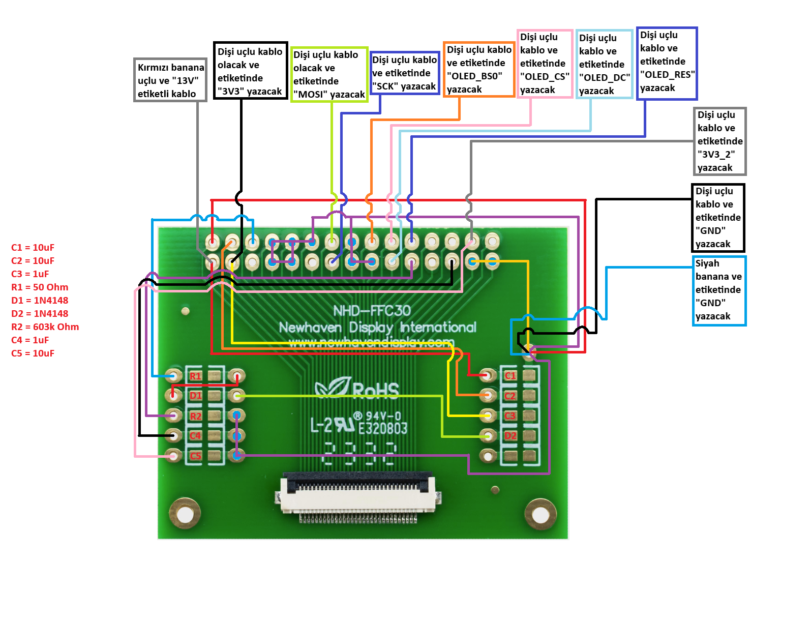
#include "main.h"
#include <string.h>
#include <stdarg.h>
#include <stdio.h>

/* Private variables ---------------------------------------------------------*/
SPI_HandleTypeDef hspi2;
UART_HandleTypeDef huart2;

/* Private function prototypes -----------------------------------------------*/
void SystemClock_Config(void);
static void MX_GPIO_Init(void);
static void MX_USART2_UART_Init(void);
static void MX_SPI2_Init(void);

/* USER CODE BEGIN 0 */

/* ===================================================================== */
/* ============ NEWHAVEN ORIJINAL KODUNUN STM32 HAL PORTU =============== */
/* ===================================================================== */

#define RED    0x0000FF
#define GREEN  0x00FF00
#define BLUE   0xFF0000
#define WHITE  0xFFFFFF
#define BLACK  0x000000

static void UART_Printf(const char* fmt, ...)
{
    char buff[128];
    va_list args;
    va_start(args, fmt);
    vsnprintf(buff, sizeof(buff), fmt, args);
    HAL_UART_Transmit(&huart2, (uint8_t*)buff, strlen(buff), HAL_MAX_DELAY);
    va_end(args);
}


static void OLED_Command_128128RGB(uint8_t c)
{
    HAL_GPIO_WritePin(SPI2_CS_GPIO_Port, SPI2_CS_Pin, GPIO_PIN_RESET);   // CS_PIN LOW
    HAL_GPIO_WritePin(OLED_DC_GPIO_Port, OLED_DC_Pin, GPIO_PIN_RESET);   // RS_PIN LOW (komut)
    HAL_SPI_Transmit(&hspi2, &c, 1, HAL_MAX_DELAY);
    HAL_GPIO_WritePin(SPI2_CS_GPIO_Port, SPI2_CS_Pin, GPIO_PIN_SET);     // CS_PIN HIGH
}

static void OLED_Data_128128RGB(uint8_t d)
{
    HAL_GPIO_WritePin(SPI2_CS_GPIO_Port, SPI2_CS_Pin, GPIO_PIN_RESET);   // CS_PIN LOW
    HAL_GPIO_WritePin(OLED_DC_GPIO_Port, OLED_DC_Pin, GPIO_PIN_SET);     // RS_PIN HIGH (veri)
    HAL_SPI_Transmit(&hspi2, &d, 1, HAL_MAX_DELAY);
    HAL_GPIO_WritePin(SPI2_CS_GPIO_Port, SPI2_CS_Pin, GPIO_PIN_SET);     // CS_PIN HIGH
}

static void OLED_SetColumnAddress_128128RGB(uint8_t x_start, uint8_t x_end)
{
    OLED_Command_128128RGB(0x15);
    OLED_Data_128128RGB(x_start);
    OLED_Data_128128RGB(x_end);
}

static void OLED_SetRowAddress_128128RGB(uint8_t y_start, uint8_t y_end)
{
    OLED_Command_128128RGB(0x75);
    OLED_Data_128128RGB(y_start);
    OLED_Data_128128RGB(y_end);
}

static void OLED_WriteMemoryStart_128128RGB(void)
{
    OLED_Command_128128RGB(0x5C);
}

static void OLED_Pixel_128128RGB(uint32_t color)
{
    OLED_Data_128128RGB((uint8_t)(color >> 16)); // R
    OLED_Data_128128RGB((uint8_t)(color >> 8));  // G
    OLED_Data_128128RGB((uint8_t)(color));       // B
}

static void OLED_FillScreen_128128RGB(uint32_t color)
{
    OLED_SetColumnAddress_128128RGB(0x00, 0x7F);
    OLED_SetRowAddress_128128RGB(0x00, 0x7F);
    OLED_WriteMemoryStart_128128RGB();
    for (int i = 0; i < 128; i++) {
        for (int j = 0; j < 128; j++) {
            OLED_Pixel_128128RGB(color);
        }
    }
}

static void OLED_Init_128128RGB(void)
{
    HAL_GPIO_WritePin(OLED_RESET_GPIO_Port, OLED_RESET_Pin, GPIO_PIN_RESET);
    HAL_Delay(300);
    HAL_GPIO_WritePin(OLED_RESET_GPIO_Port, OLED_RESET_Pin, GPIO_PIN_SET);
    HAL_Delay(10);

    OLED_Command_128128RGB(0xFD); // Command lock setting
    OLED_Data_128128RGB(0x12);    // unlock
    OLED_Command_128128RGB(0xFD); // Command lock setting
    OLED_Data_128128RGB(0xB1);    // unlock
    OLED_Command_128128RGB(0xAE); // Set Display OFF
    OLED_Command_128128RGB(0xB3); // Set Display Clock Divide Ratio
    OLED_Data_128128RGB(0xF1);
    OLED_Command_128128RGB(0xCA); // Set MUX ratio
    OLED_Data_128128RGB(0x7F);
    OLED_Command_128128RGB(0xA2); // Set Display offset
    OLED_Data_128128RGB(0x00);
    OLED_Command_128128RGB(0xA1); // Set display start line
    OLED_Data_128128RGB(0x00);
    OLED_Command_128128RGB(0xA0); // Set Re-map, color depth
    OLED_Data_128128RGB(0xB4);
    OLED_Command_128128RGB(0xB5); // set GPIO
    OLED_Data_128128RGB(0x00);
    OLED_Command_128128RGB(0xAB); // Function Set
    OLED_Data_128128RGB(0x01);
    OLED_Command_128128RGB(0xB4); // Set Segment Low Voltage
    OLED_Data_128128RGB(0xA0);
    OLED_Data_128128RGB(0xB5);
    OLED_Data_128128RGB(0x55);
    OLED_Command_128128RGB(0xC1); // Set Contrast Current
    OLED_Data_128128RGB(0xC8);
    OLED_Data_128128RGB(0x80);
    OLED_Data_128128RGB(0xC8);
    OLED_Command_128128RGB(0xC7); // Master Contrast Current Control
    OLED_Data_128128RGB(0x0F);
    OLED_Command_128128RGB(0xB9); // use linear grayscale LUT
    OLED_Command_128128RGB(0xB1); // Set Phase Length
    OLED_Data_128128RGB(0x32);
    OLED_Command_128128RGB(0xBB); // Set Pre-charge Voltage
    OLED_Data_128128RGB(0x17);
    OLED_Command_128128RGB(0xB2); // Display enhancement
    OLED_Data_128128RGB(0xA4);
    OLED_Data_128128RGB(0x00);
    OLED_Data_128128RGB(0x00);
    OLED_Command_128128RGB(0xB6); // Set Second Pre-charge Period
    OLED_Data_128128RGB(0x01);
    OLED_Command_128128RGB(0xBE); // Set VCOMH
    OLED_Data_128128RGB(0x05);
    OLED_Command_128128RGB(0xA6); // Normal display

    // oled_Clear_Screen(): datasheet sirasina gore Display ON'dan ONCE calisir
    OLED_FillScreen_128128RGB(BLACK);

    OLED_Command_128128RGB(0xAF); // Set Display ON
    HAL_Delay(200);
    OLED_Command_128128RGB(0x5C); // Enable Write to RAM command
}

static void OLED_TestLoop(void)
{
    OLED_FillScreen_128128RGB(RED);
    HAL_Delay(1000);

    OLED_FillScreen_128128RGB(GREEN);
    HAL_Delay(1000);

    OLED_FillScreen_128128RGB(BLUE);
    HAL_Delay(1000);

    OLED_FillScreen_128128RGB(WHITE);
    HAL_Delay(1000);

    OLED_FillScreen_128128RGB(BLACK);

    OLED_SetColumnAddress_128128RGB(0x00, 0x7F);
    OLED_SetRowAddress_128128RGB(0x00, 0x7F);
    OLED_WriteMemoryStart_128128RGB();
    for (int y = 0; y < 128; y++) {
        for (int x = 0; x < 128; x++) {
            if (x == 0 || x == 127 || y == 0 || y == 127) {
                OLED_Pixel_128128RGB(RED);
            } else {
                OLED_Pixel_128128RGB(BLACK);
            }
        }
    }
}

/* USER CODE END 0 */

int main(void)
{
  HAL_Init();
  SystemClock_Config();

  MX_GPIO_Init();
  MX_USART2_UART_Init();
  MX_SPI2_Init();

  /* USER CODE BEGIN 2 */
  UART_Printf("Baslatiliyor (Newhaven orijinal init dizisi)...\r\n");

  OLED_Init_128128RGB();
  OLED_Command_128128RGB(0xAE);
  HAL_Delay(3000);
  OLED_Command_128128RGB(0xA5);
  UART_Printf("Init tamamlandi.\r\n");
  /* USER CODE END 2 */

  while (1)
  {
    /* USER CODE BEGIN WHILE */
    OLED_TestLoop();
    HAL_Delay(2000);
    /* USER CODE END WHILE */
  }
}

/**
  * @brief System Clock Configuration
  */
void SystemClock_Config(void)
{
  RCC_OscInitTypeDef RCC_OscInitStruct = {0};
  RCC_ClkInitTypeDef RCC_ClkInitStruct = {0};
  RCC_PeriphCLKInitTypeDef PeriphClkInit = {0};

  RCC_OscInitStruct.OscillatorType = RCC_OSCILLATORTYPE_HSI;
  RCC_OscInitStruct.HSIState = RCC_HSI_ON;
  RCC_OscInitStruct.HSICalibrationValue = RCC_HSICALIBRATION_DEFAULT;
  RCC_OscInitStruct.PLL.PLLState = RCC_PLL_ON;
  RCC_OscInitStruct.PLL.PLLSource = RCC_PLLSOURCE_HSI;
  RCC_OscInitStruct.PLL.PLLMUL = RCC_PLL_MUL9;
  RCC_OscInitStruct.PLL.PREDIV = RCC_PREDIV_DIV1;
  if (HAL_RCC_OscConfig(&RCC_OscInitStruct) != HAL_OK)
  {
    Error_Handler();
  }

  RCC_ClkInitStruct.ClockType = RCC_CLOCKTYPE_HCLK|RCC_CLOCKTYPE_SYSCLK
                              |RCC_CLOCKTYPE_PCLK1|RCC_CLOCKTYPE_PCLK2;
  RCC_ClkInitStruct.SYSCLKSource = RCC_SYSCLKSOURCE_PLLCLK;
  RCC_ClkInitStruct.AHBCLKDivider = RCC_SYSCLK_DIV1;
  RCC_ClkInitStruct.APB1CLKDivider = RCC_HCLK_DIV2;
  RCC_ClkInitStruct.APB2CLKDivider = RCC_HCLK_DIV1;

  if (HAL_RCC_ClockConfig(&RCC_ClkInitStruct, FLASH_LATENCY_1) != HAL_OK)
  {
    Error_Handler();
  }
  PeriphClkInit.PeriphClockSelection = RCC_PERIPHCLK_USART2;
  PeriphClkInit.Usart2ClockSelection = RCC_USART2CLKSOURCE_PCLK1;
  if (HAL_RCCEx_PeriphCLKConfig(&PeriphClkInit) != HAL_OK)
  {
    Error_Handler();
  }
}

static void MX_SPI2_Init(void)
{
  hspi2.Instance = SPI2;
  hspi2.Init.Mode = SPI_MODE_MASTER;
  hspi2.Init.Direction = SPI_DIRECTION_2LINES;
  hspi2.Init.DataSize = SPI_DATASIZE_8BIT;
  hspi2.Init.CLKPolarity = SPI_POLARITY_LOW;
  hspi2.Init.CLKPhase = SPI_PHASE_1EDGE;
  hspi2.Init.NSS = SPI_NSS_SOFT;
  hspi2.Init.BaudRatePrescaler = SPI_BAUDRATEPRESCALER_256;
  hspi2.Init.FirstBit = SPI_FIRSTBIT_MSB;
  hspi2.Init.TIMode = SPI_TIMODE_DISABLE;
  hspi2.Init.CRCCalculation = SPI_CRCCALCULATION_DISABLE;
  hspi2.Init.CRCPolynomial = 7;
  hspi2.Init.CRCLength = SPI_CRC_LENGTH_DATASIZE;
  hspi2.Init.NSSPMode = SPI_NSS_PULSE_DISABLE;
  if (HAL_SPI_Init(&hspi2) != HAL_OK)
  {
    Error_Handler();
  }
}

/**
  * @brief USART2 Initialization Function
  */
static void MX_USART2_UART_Init(void)
{
  huart2.Instance = USART2;
  huart2.Init.BaudRate = 38400;
  huart2.Init.WordLength = UART_WORDLENGTH_8B;
  huart2.Init.StopBits = UART_STOPBITS_1;
  huart2.Init.Parity = UART_PARITY_NONE;
  huart2.Init.Mode = UART_MODE_TX_RX;
  huart2.Init.HwFlowCtl = UART_HWCONTROL_NONE;
  huart2.Init.OverSampling = UART_OVERSAMPLING_16;
  huart2.Init.OneBitSampling = UART_ONE_BIT_SAMPLE_DISABLE;
  huart2.AdvancedInit.AdvFeatureInit = UART_ADVFEATURE_NO_INIT;
  if (HAL_UART_Init(&huart2) != HAL_OK)
  {
    Error_Handler();
  }
}

/**
  * @brief GPIO Initialization Function
  */
static void MX_GPIO_Init(void)
{
  GPIO_InitTypeDef GPIO_InitStruct = {0};

  __HAL_RCC_GPIOC_CLK_ENABLE();
  __HAL_RCC_GPIOF_CLK_ENABLE();
  __HAL_RCC_GPIOA_CLK_ENABLE();
  __HAL_RCC_GPIOB_CLK_ENABLE();

  HAL_GPIO_WritePin(LD2_GPIO_Port, LD2_Pin, GPIO_PIN_RESET);
  HAL_GPIO_WritePin(GPIOB, SPI2_CS_Pin|OLED_DC_Pin|OLED_RESET_Pin, GPIO_PIN_RESET);

  GPIO_InitStruct.Pin = B1_Pin;
  GPIO_InitStruct.Mode = GPIO_MODE_IT_FALLING;
  GPIO_InitStruct.Pull = GPIO_NOPULL;
  HAL_GPIO_Init(B1_GPIO_Port, &GPIO_InitStruct);

  GPIO_InitStruct.Pin = LD2_Pin;
  GPIO_InitStruct.Mode = GPIO_MODE_OUTPUT_PP;
  GPIO_InitStruct.Pull = GPIO_NOPULL;
  GPIO_InitStruct.Speed = GPIO_SPEED_FREQ_LOW;
  HAL_GPIO_Init(LD2_GPIO_Port, &GPIO_InitStruct);

  GPIO_InitStruct.Pin = SPI2_CS_Pin|OLED_DC_Pin|OLED_RESET_Pin;
  GPIO_InitStruct.Mode = GPIO_MODE_OUTPUT_PP;
  GPIO_InitStruct.Pull = GPIO_NOPULL;
  GPIO_InitStruct.Speed = GPIO_SPEED_FREQ_LOW;
  HAL_GPIO_Init(GPIOB, &GPIO_InitStruct);
}

void Error_Handler(void)
{
  __disable_irq();
  while (1)
  {
  }
}