Subject: LM335AZ lead root copper exposure inquiry
This account only shares restored community content posted by members between May 22 and June 9, 2026, who did not register for the new community.
[Moderation: To get answers from the English-speaking community, it is helpful to ask in English as well. I have therefore translated your text using a web-based tool]
Dear STMicroelectronics Support Team,
I hope this email finds you well.
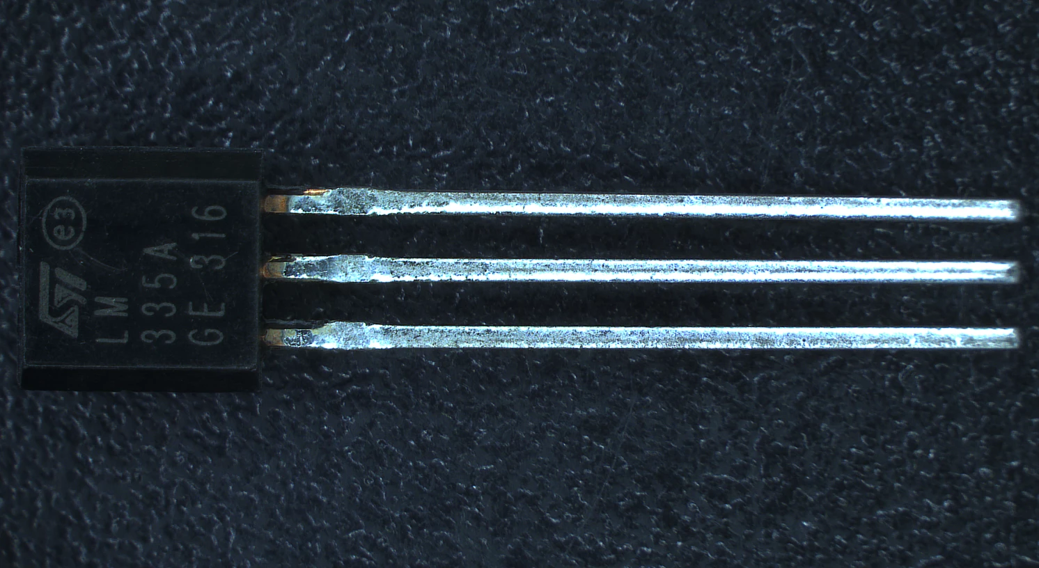
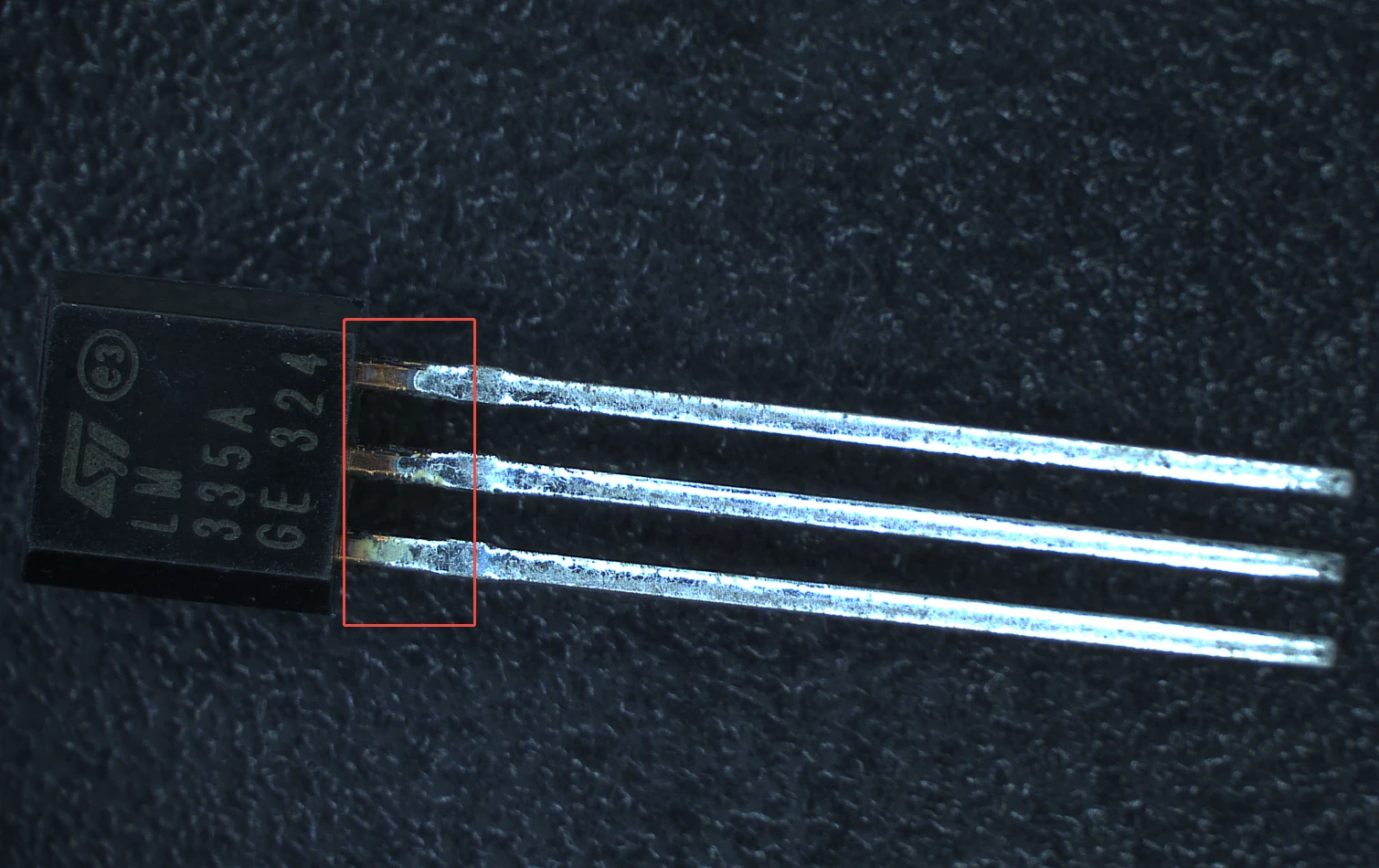
We are currently investigating a specific appearance issue concerning the LM335AZ in the TO-92 package. Recently, we have observed some defects at the base of the leads, in particular some copper lead exposure/oxidation. Based on our preliminary assessment, this appears to be a natural result of the lead-forming or assembly process.
However, after carefully reviewing the official ST datasheet and technical documentation, we were unable to find any formal or stated specification for a specific process relating to this phenomenon.
To ensure our quality control is fully clear and to address enquiries from downstream customers, we would be grateful if STMicroelectronics could provide an official statement, declaration, or formal response regarding this appearance issue, confirming whether it falls within STMicroelectronics’ standard manufacturing tolerances and whether it does not affect the component’s reliability or electrical performance.
I have attached high-resolution photographs of the affected area for your reference.
Thank you very much for your time, support, and professional assistance. I look forward to your satisfactory reply.
Yours faithfully,
亲爱的意法半导体支持团队,
我希望这封电子邮件能让您满意。
我们目前正在跟踪有关LM335AZ(TO-92封装)的特定外观。最近,我们在引线根部观察到了一些缺陷,特别是一些铜引线/氧化。根据我们的初步估计,这似乎是引线成型或整机制造过程的自然结果。
然而,在仔细查阅ST官方数据表和技术文档后,我们发现了任何针对这一现象的特定工艺的正式或声明规范。
为了确保我们的质量控制完全清楚并解决下游客户的询问,如果意法半导体能够就该外观事件提供官方声明、声明或正式答复(确认其是否在意法半导体的标准制造公差范围内,并且不会影响组件的可靠性或电气性能),我们将不胜感激。
我附上了该地点的高清照片供您参考。
非常感谢您的时间、支持和专业帮助。我期待您的满意答复。
在此致,