

Associate
July 20, 2026
Question

Only receiving FF out of the M95M04

  • July 20, 2026
  • 4 replies
  • 94 views

Hello,

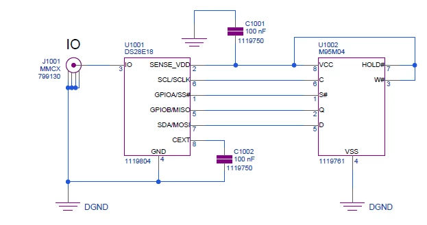
I am trying to use the M95M04 as a SPI slave device from the ADI DS28E18 one-wire bridge. A picture has been uploaded to show the entire hardware setup. My main issue is that whenever I try to send data to the EEprom and then read that data back, I only get FF as a result. When setting write enable or write disable, the MISO line pulls low like would be expected and returns 00. I have used an oscilloscope with a bus decoder to ensure that the correct commands are being sent out of the DS28E18 to the M95M04, and they are. We never see the WIP bit go high, and we have tried many changes in both the hardware and the software. Our current hardware setup is based off of the schematic image I have posted, but there have been some modifications. C1001 has been changed to 10uF X7R, C1002 has been changed to 1uF X7R, and 10k pull-up resistors have been added on the S# and D pins. From the software side, I have attached the code that our software engineer is using. I have tried replacing the EEprom, I have confirmed that the layout on our board is correct, and I have ensured the traces between the DS28E18 and M95M04 are all intact. If someone could please look through our setup and see if there are any obvious flaws that would be fantastic.

The driver that we are using is linked here: github.com/DRNadler/1Wire.git
static int do_jedec_id(void)
{
uint8_t seq[64];
uint8_t rx[16];
size_t i = 0;
unsigned short seq_addr;
uint8_t status;

if (init_ds28(1) != 0)
return 1;

if (ds28_prepare_spi() != 0)
return 1;

printf("STEP 1: Initial status\n");

if (read_eeprom_status_byte(&status) != 0)
return 1;

printf("Status = 0x%02X\n", status);

printf("STEP 2: WREN\n");

if (write_enable_only() != 0)
return 1;

if (read_eeprom_status_byte(&status) != 0)
return 1;

printf("Status after WREN = 0x%02X\n", status);

printf("STEP 3: RDID\n");

seq[i++] = DS28_SPI_SS_LOW;

seq[i++] = DS28_SPI_WR_RD_BYTE;
seq[i++] = 4U; /* write length */
seq[i++] = 16U; /* read length */

seq[i++] = M95_CMD_RDID; /* 0x83 */
seq[i++] = 0x00;
seq[i++] = 0x00;
seq[i++] = 0x00;

/*
* Save where read data begins.
* For WR_RD_BYTE the returned bytes overwrite
* the dummy bytes in sequencer memory.
*/
seq_addr = (unsigned short)i;

for (int j = 0; j < 16; j++)
{
seq[i++] = 0xFF;
}

seq[i++] = DS28_SPI_SS_HIGH;

dump_bytes_limited("RDID SEQ",
seq,
i,
64);

if (!DS28E18_WriteSequencer(0U, seq, (int)i))
{
fprintf(stderr,
"DS28E18_WriteSequencer failed\n");
return 1;
}

if (!DS28E18_RunSequencer(0U, (unsigned short)i))
{
fprintf(stderr,
"DS28E18_RunSequencer failed\n");
return 1;
}

memset(rx, 0, sizeof(rx));

if (!DS28E18_ReadSequencer(seq_addr,
rx,
sizeof(rx)))
{
fprintf(stderr,
"DS28E18_ReadSequencer failed\n");
return 1;
}

dump_bytes_limited("RDID RX",
rx,
sizeof(rx),
64);

if (read_eeprom_status_byte(&status) != 0)
return 1;

printf("Status after RDID = 0x%02X\n", status);

printf("WIP=%u WEL=%u\n",
(status & M95_STATUS_WIP_MASK) ? 1U : 0U,
(status & M95_STATUS_WEL_MASK) ? 1U : 0U);

return 0;
}

This code is an example of something that we have that only returns FF from the M95M04

4 replies

stevc_26Author
Associate
July 20, 2026

Here is the full one-wire communication chain: 


Peter BENSCH
ST Technical Moderator
July 27, 2026

Welcome ​​@stevc_26, to the community!

The code structure looks broadly reasonable, but two things stand out:

  • W# is tied to VCC in the schematic, which can block writes entirely
  • the EEPROM may still be mis-powered or not selected correctly during the SPI transaction

Also, I would strongly suggest logging the DS28E18 result/status byte after each sequencer run, not just the SPI payload. Additionally, I recommend replacing C1002 (100nF) with a 470nF capacitor, as mentioned on page 2 of the DS28E18 datasheet.

I have only looked at your code snippet here, (for time reasons) however not your project on Git, so please:

  1. Check read and log the status of DS28E18 in do_jedec_id() after the RunSequencer
  2. Check in read_eeprom_status_byte() and write_enable_only()
    • exact byte sequence
    • sent dummy bytes
    • CS timing
    • number of reads
  3. Measure SENS_VDD, not just infer it logically

Hope that helps?

Regards
/Peter

In order to give better visibility on the answered topics, please click on Accept as Solution on the reply which solved your issue or answered your question.
Visitor II
July 30, 2026

1. Primary Issue: DS28E18 Sequencer Data Offset & Length Misconfiguration

Looking closely at your sequencer construction for RDID:


seq[i++] = DS28_SPI_SS_LOW;

seq[i++] = DS28_SPI_WR_RD_BYTE;
seq[i++] = 4U;      /* write length */
seq[i++] = 16U;     /* read length  */

seq[i++] = M95_CMD_RDID;   /* 0x83 */
seq[i++] = 0x00;
seq[i++] = 0x00;
seq[i++] = 0x00;

/* Save where read data begins */
seq_addr = (unsigned short)i; 

for (int j = 0; j < 16; j++) {
    seq[i++] = 0xFF;
}

seq[i++] = DS28_SPI_SS_HIGH;


Problem A: M95M04 RDID Command & Address Structure

The M95M04 uses 3-byte addressing (24-bit address) for standard memory read/write commands (0x03 / 0x02), but for Read Identification (RDID - 0x83), the instruction format consists of:

  • 1-byte Command (0x83)

  • 3 Dummy Address Bytes (0x00 0x00 0x00) OR depending on the specific M95M04 datasheet variant, RDID expects 3 address bytes pointing to the Identification Page start (e.g., 0x00 0x00 0x00), followed by clocking out the data.

Problem B: DS28E18 Buffer Index Misalignment

In the DS28E18 SPI_WR_RD_BYTE command structure:

  1. Write Length = 4 means it transmits the next 4 bytes in the buffer (0x83, 0x00, 0x00, 0x00).

  2. Read Length = 16 means it immediately continues clocking out 16 dummy cycles and populates the DS28E18 internal buffer starting from the location where the write payload began (or from the start of the sequencer response buffer depending on the DS28E18 driver implementation).

When you call:

DS28E18_ReadSequencer(seq_addr, rx, sizeof(rx));


If your DS28E18_ReadSequencer function reads back from the DS28E18 memory, seq_addr is pointing to byte offset i after the command payload. Depending on how 1Wire.git handles the sequencer buffer mapping, the DS28E18 stores returned bytes starting at the beginning of the transmit payload offset inside the internal SRAM buffer.

  • Fix: Verify if DS28E18_ReadSequencer needs to read starting at seq_addr - 4 or at the base address of DS28_SPI_WR_RD_BYTE.

2. SPI Mode & Clock Polarity/Phase Mismatch

The M95M04 supports SPI Mode 0 (CPOL=0, CPHA=0) and SPI Mode 3 (CPOL=1, CPHA=1).

  1. Ensure the DS28E18 SPI configuration command (ds28_prepare_spi()) explicitly configures SPI Mode 0 or Mode 3.

  2. If the DS28E18 is defaulting to Mode 1 or Mode 2, the M95M04 will sample bits on the wrong clock edge, causing all reads to shift or fail back to the default 0xFF state (since MISO stays un-driven / high impedance).

3. Hardware & Power Considerations

A. Powering the M95M04 from SENSE_VDD

In your schematic, SENSE_VDD (Pin 2 of U1001 DS28E18) is driving VCC (Pin 8 of U1002 M95M04).

  • Power Delivery Limit: The DS28E18 SENSE_VDD pin delivers internal power derived from the 1-Wire parasitic / IO line. The current output capability of SENSE_VDD is very limited (typically around 1 mA to a few mA max depending on 1-Wire strong pull-up).

  • M95M04 Current Consumption: The M95M04 (4 Mbit EEPROM) can consume up to 3 mA to 5 mA during write cycles and around 2 mA during active SPI reads.

  • If VCC sags below the minimum operating voltage of the M95M04 (typically 1.8V to 2.5V depending on suffix) during high-frequency SPI clocking, the EEPROM logic resets, resulting in 0xFF output.

Recommended Test: Supply VCC of the M95M04 directly from a dedicated external power supply (3.3V) rather than SENSE_VDD to rule out power collapse.

B. Pull-Up Resistors

  • Adding 10kΩ pull-ups on S# (CS) and D (MOSI) was a good change.

  • Ensure W# (Pin 3) and HOLD# (Pin 7) are strongly tied to VCC (which you have done in the schematic).

  • Verify that S# (Chip Select) goes fully HIGH between separate sequencer transactions. The M95M04 requires a High-to-Low transition on S# to reset its internal SPI state machine for every new command.

4. Troubleshooting Checklist

  1. Test Standard Read (0x03): Instead of RDID (0x83), try reading standard memory address 0x000000 using command 0x03.

    • Send: [0x03, 0x00, 0x00, 0x00]

    • Write Length: 4, Read Length: 4

  2. Measure VCC with an Oscilloscope: Probe VCC on the M95M04 while running the sequencer script. Ensure it does not dip or drop below operating threshold when S# goes LOW.

  3. Verify SPI Clock Speed: Set the DS28E18 SPI clock divider to its slowest speed (e.g., 100 kHz - 1 MHz) during testing to minimize power draw from SENSE_VDD.

stevc_26Author
Associate
August 4, 2026

Thanks everyone for your suggestions! The software engineer and I have now tried most of these, but we still have the same issue. We ended up getting DS28E18 and M95M04 eval kits and testing using those. Even using the DS28E18 software and powering the m95m04 from an external 3.3V yields the same results from the SPI transactions. We are looking into getting a different eeprom model to test with.

Here is an image of what we are reading back in the ADI software: