
Design Review BQ40Z80 BMS
Hello am designing a 6S battery pack (25 V nominal) around the BQ40Z80 and would appreciate your feedback on my schematic before I proceed to layout. I used the BQ40Z80 EVM reference design (datasheet Figure 7-1) as a starting point and adapted it for a higher current.
Design summary
-
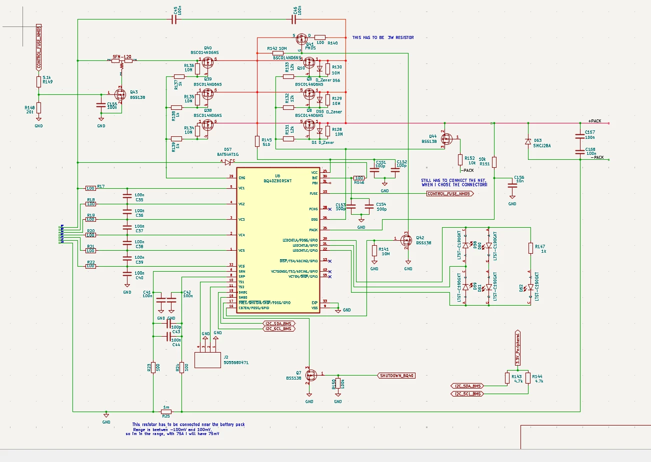
Cells: 6S (VC1–VC6), with 100 Ω / 100 nF RC filters on each cell input.
- Current: 60 A continuous, 80 A peak (the charge current is lower).
- Current sense: 1 mΩ shunt on SRP/SRN, which gives about 75 mV at 75 A. This is within the ±100 mV input range of the device.
- Protection FETs: 3× BSC014N06NS in parallel on the CHG side and 3× in parallel on the DSG side, in a common-drain back-to-back configuration.
- Gate drive: single gate resistors per FET (1 kΩ on the CHG side, 12 kΩ on the DSG side), 10 MΩ gate-source resistors, and clamps on the gate-source of the DSG FETs.
- Pre-charge/pre-discharge: P-channel MOSFET (Q41) in series with a 100 Ω / 3 W resistor (R140), driven by a BSS138 from LEDCNTLA (PCHG is not used).
- Fuse: the FUSE pin goes to a net called CONTROL_FUSE_NMOS, which drives an NMOS (BSS138) that triggers the heater fuse.
- Communication: SMBus/I2C on SMBC/SMBD with 4.7 kΩ pull-ups to 3.3 V, plus an SHUTDOWN_BQ40 line driven by a BSS138 ( here i got a question, i should put a pull-up or not?)
Questions
1. FET drive: Is it acceptable to drive three parallel FETs per side with the CHG and DSG pins, given the total gate charge? Do you recommend lower gate resistors or a dedicated gate driver, and what turn-on/turn-off times do you consider safe at 80 A?
2. the SHUTDOWN PIN requires a pull up or not? on the datasheet It says do not pull-up this PIN but it seems refered to when you use it as DISP
3. the battery afterwards will power supply 4 motors, i should put the tvs as close as possible to the 2 N series FET or to pack+?
4. the tvs has to have GND or pack- as reference?
5. The mosfet Q44 drain has to be connected to PACK- or GND and why? ( consider that this FET is usef for reverse voltage protection )
I have attached the schematic as an image. If it would help, I can also share the full project files
Thank you very much for your time and support.
Best regards