LSM6DSV80X Development (1) — Reading Gyroscope Data in Polling Mode
Overview
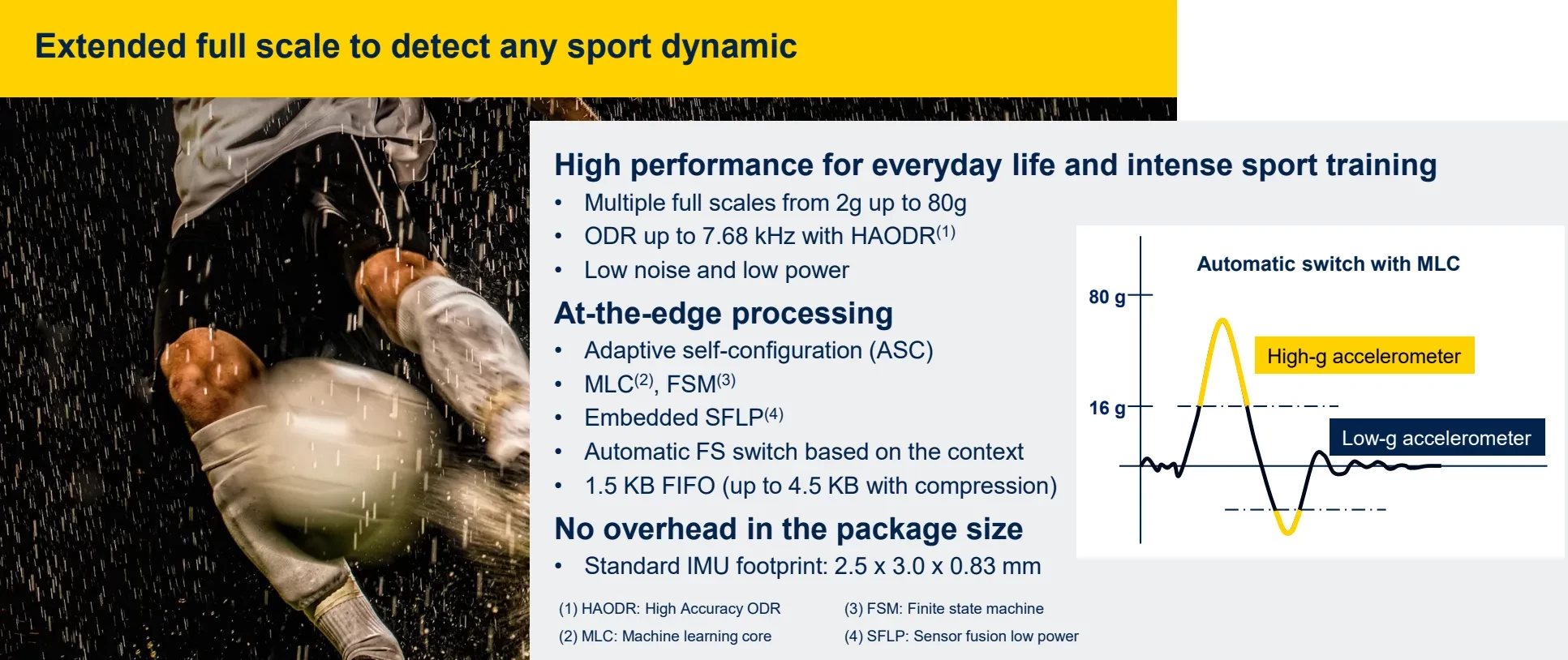
The LSM6DSV80X represents a breakthrough in wearable technology. Its ability to measure both high- and low-acceleration ranges, combined with high energy efficiency and advanced processing capabilities, makes it an ideal choice for users who need detailed data analysis and improved performance tracking in high-impact sports and activities such as volleyball, football, tennis, boxing, and explosive jumping.
This IMU provides a comprehensive solution for wearable devices, high-impact detection, and activity tracking, delivering an excellent combination of accuracy, integration, and efficiency.
The LSM6DSV80X is the world’s first IMU to combine high-g acceleration measurement of up to 80 g and low-g sensing capabilities in a single package. It integrates advanced features, including edge processing and sensor fusion, to provide consistent performance and valuable data for sports-wearable tracking and high-impact detection.

The device supports edge AI capabilities, using a finite state machine (FSM) for configurable motion tracking and a machine learning core (MLC) for context awareness. It also provides exportable AI functions for wearable applications.
The LSM6DSV80X supports the Adaptive Self-Configuration (ASC) function, which allows the device to be automatically reconfigured in real time according to the detection of specific motion patterns or the output of a decision tree configured in the MLC, without any intervention from the host processor.
Hardware Preparation
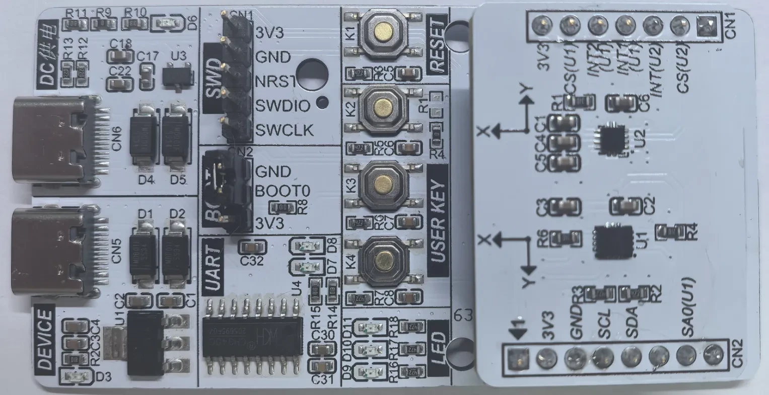
First, prepare a development board. In this example, I use a development board designed by myself. Those who need the board may apply for one.
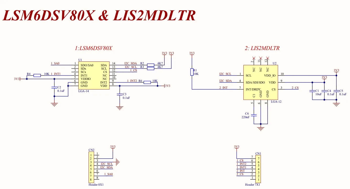
The main controller is the STM32H503CB, the IMU is the LSM6DSV80X, and the magnetometer is the LIS2MDL.
Reference Program
https://github.com/CoreMaker-lab/LSM6DSV80X
Generating the Project with STM32CubeMX
Use STM32CubeMX to generate the example project. The MCU used in this project is the STM32H503CB.
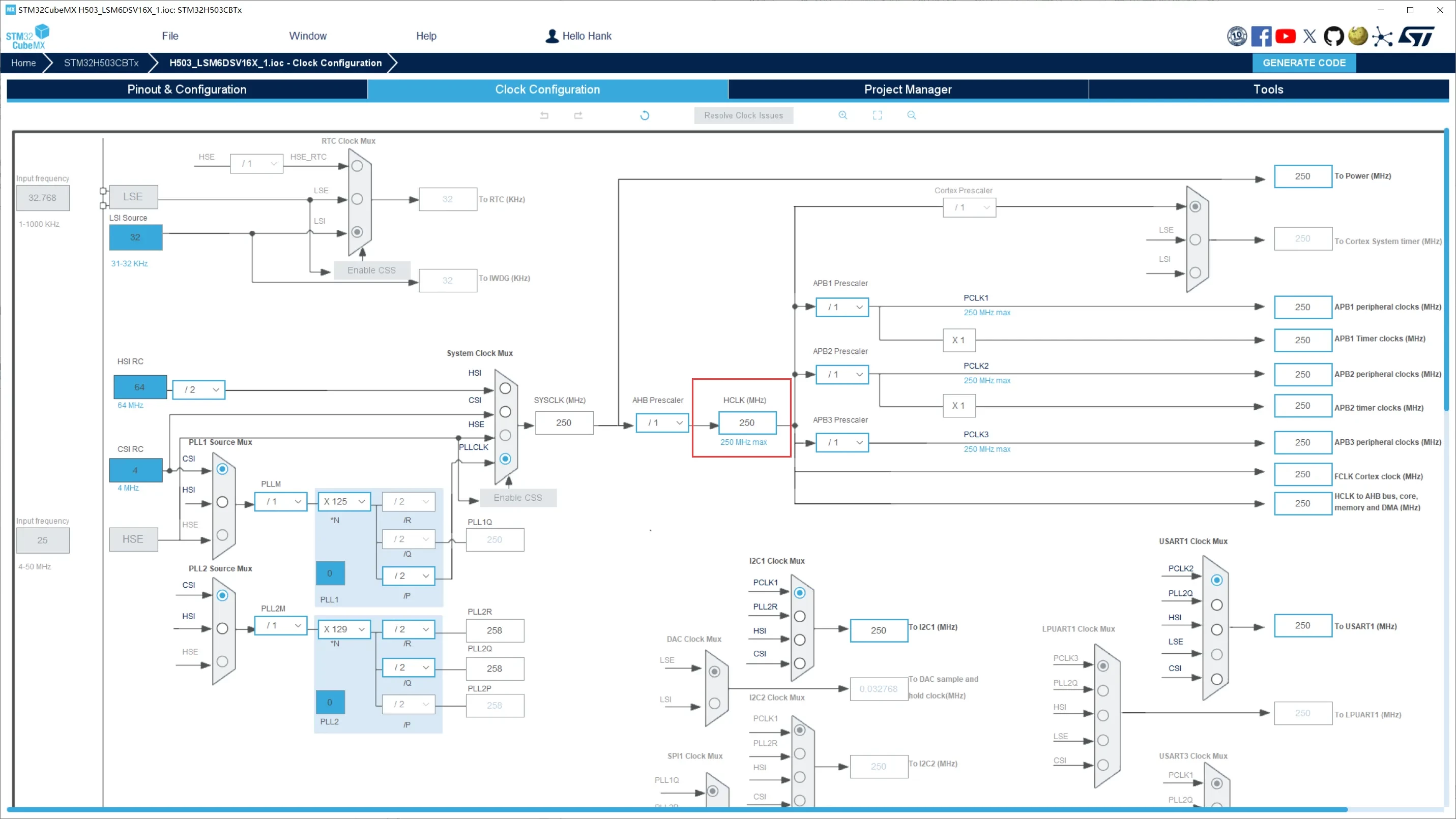
Configure the clock tree and set the system clock frequency to 250 MHz.
UART Configuration
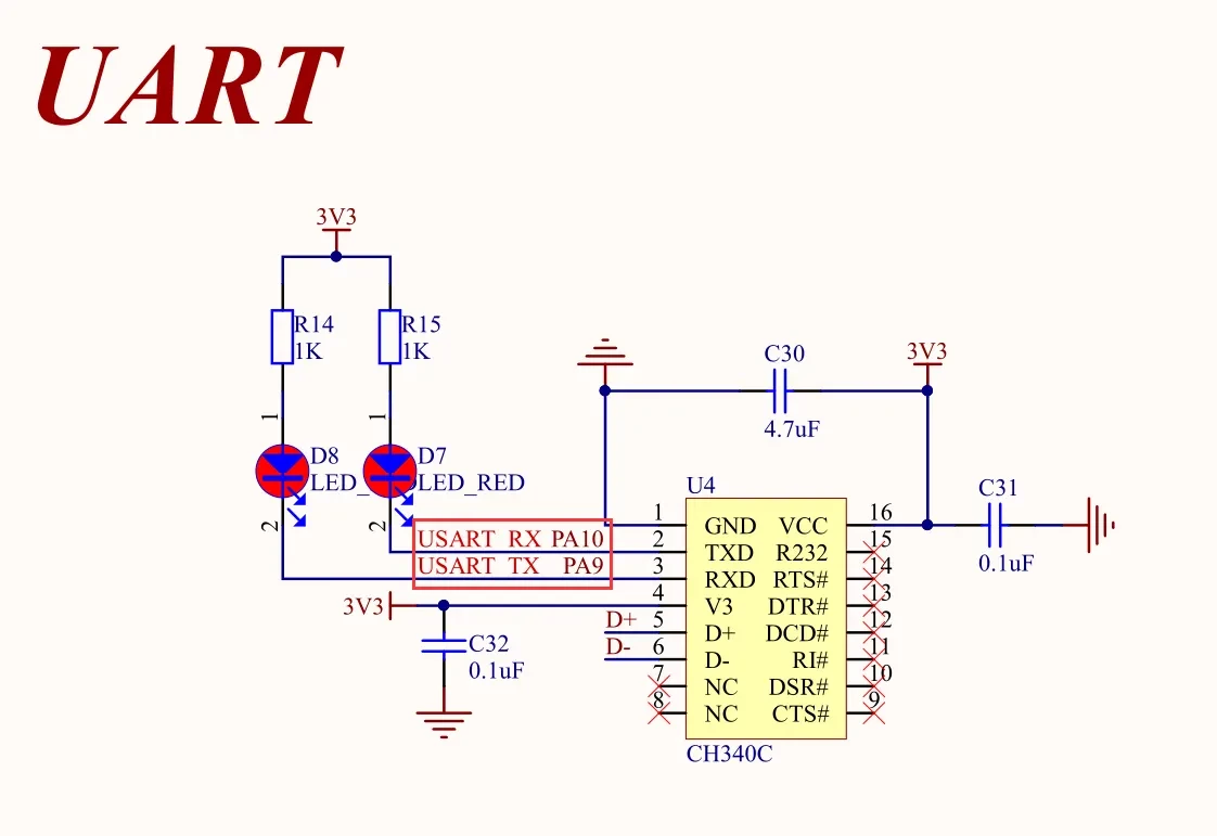
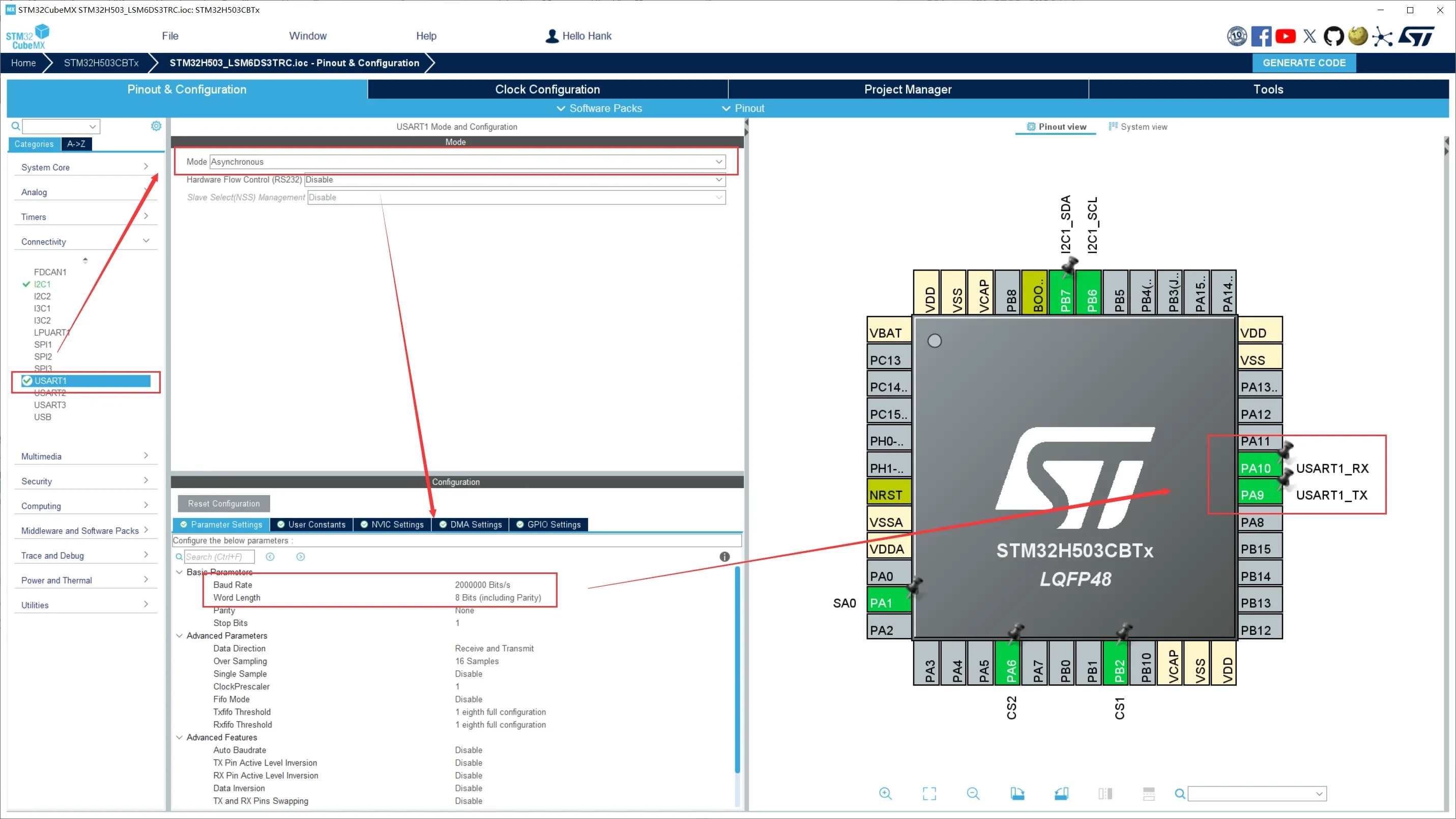
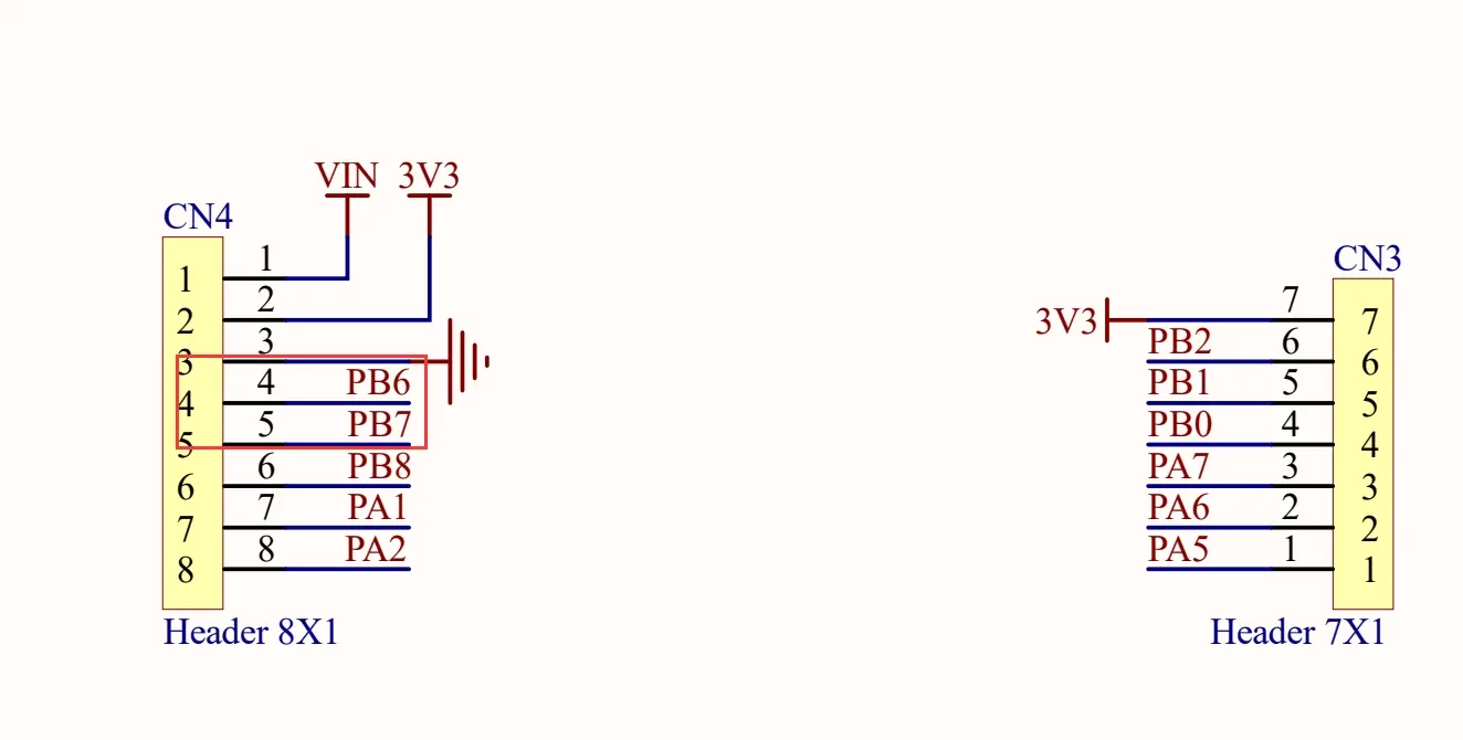
According to the schematic, PA9 and PA10 are connected to the development board’s UART interface.
Configure the UART baud rate to 2,000,000 bps.
Communication Interface
The LSM6DSV80X supports both SPI and I²C communication interfaces.
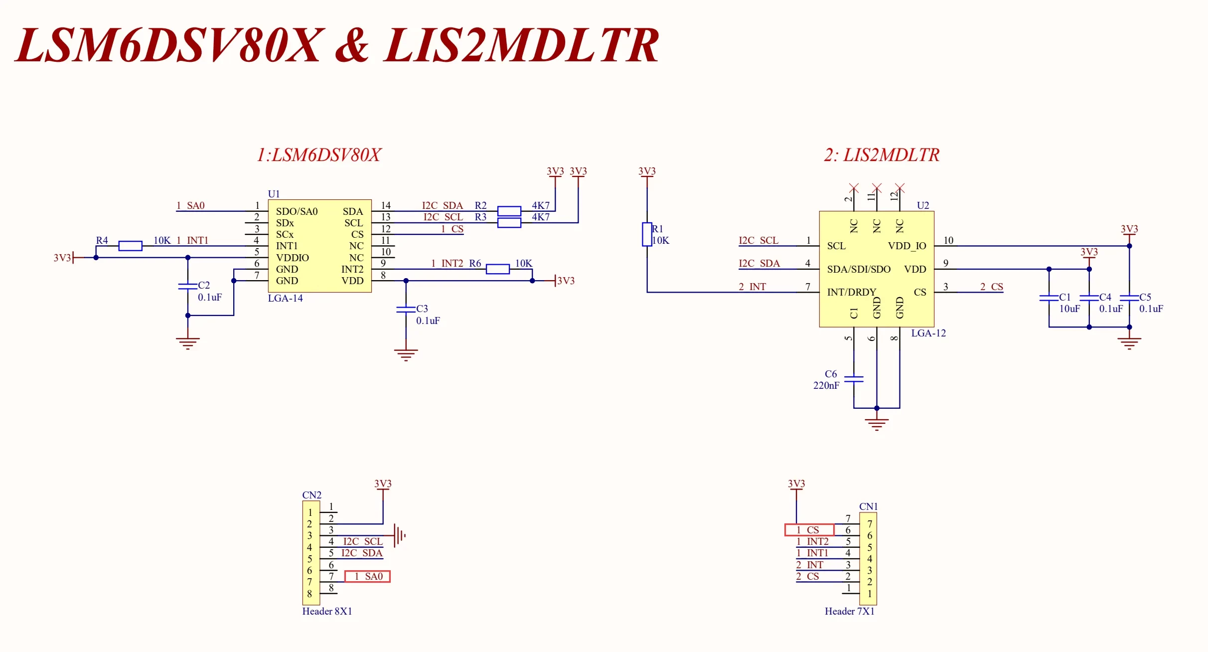
The minimum system circuit is shown below.
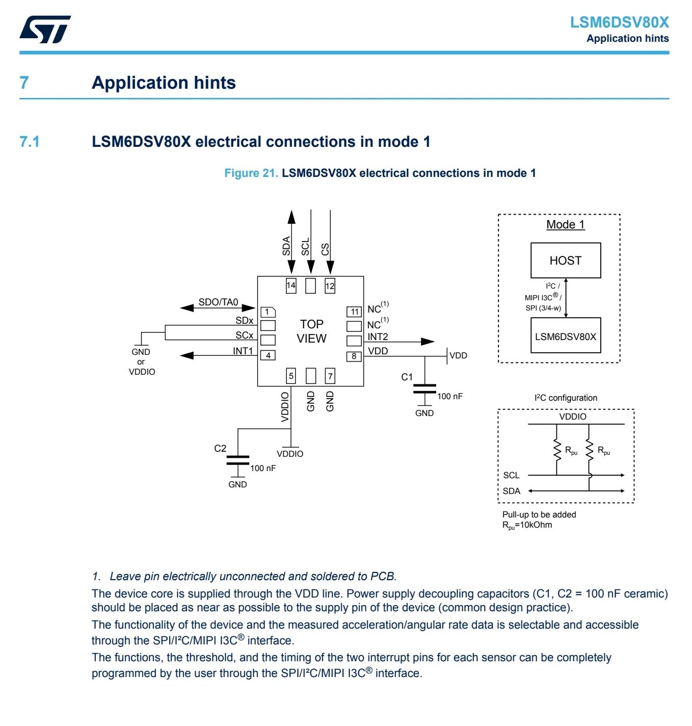
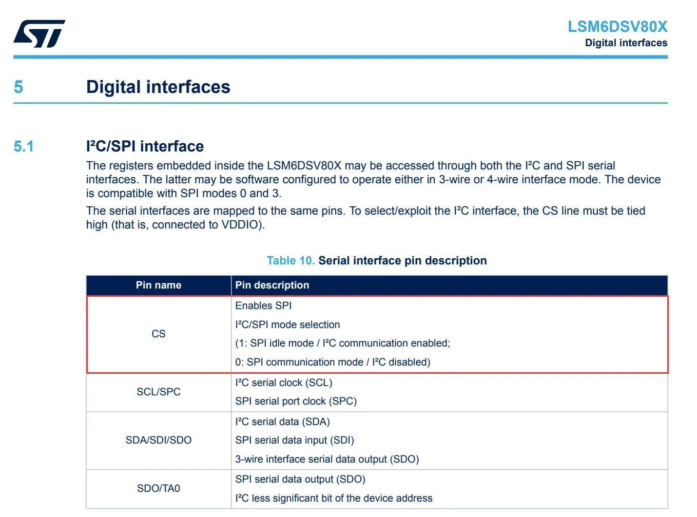
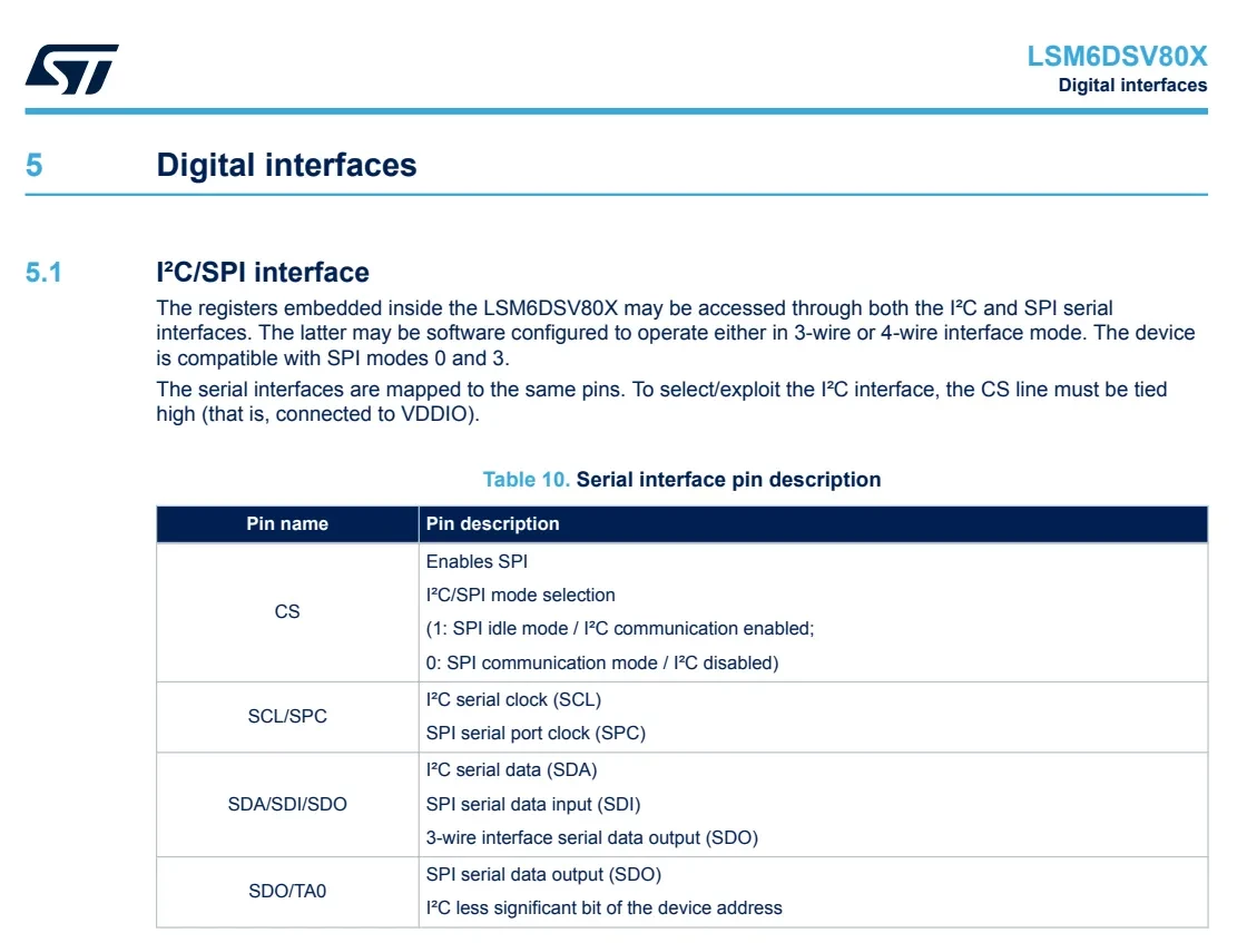
When the CS pin is pulled high, the device operates in I²C mode.
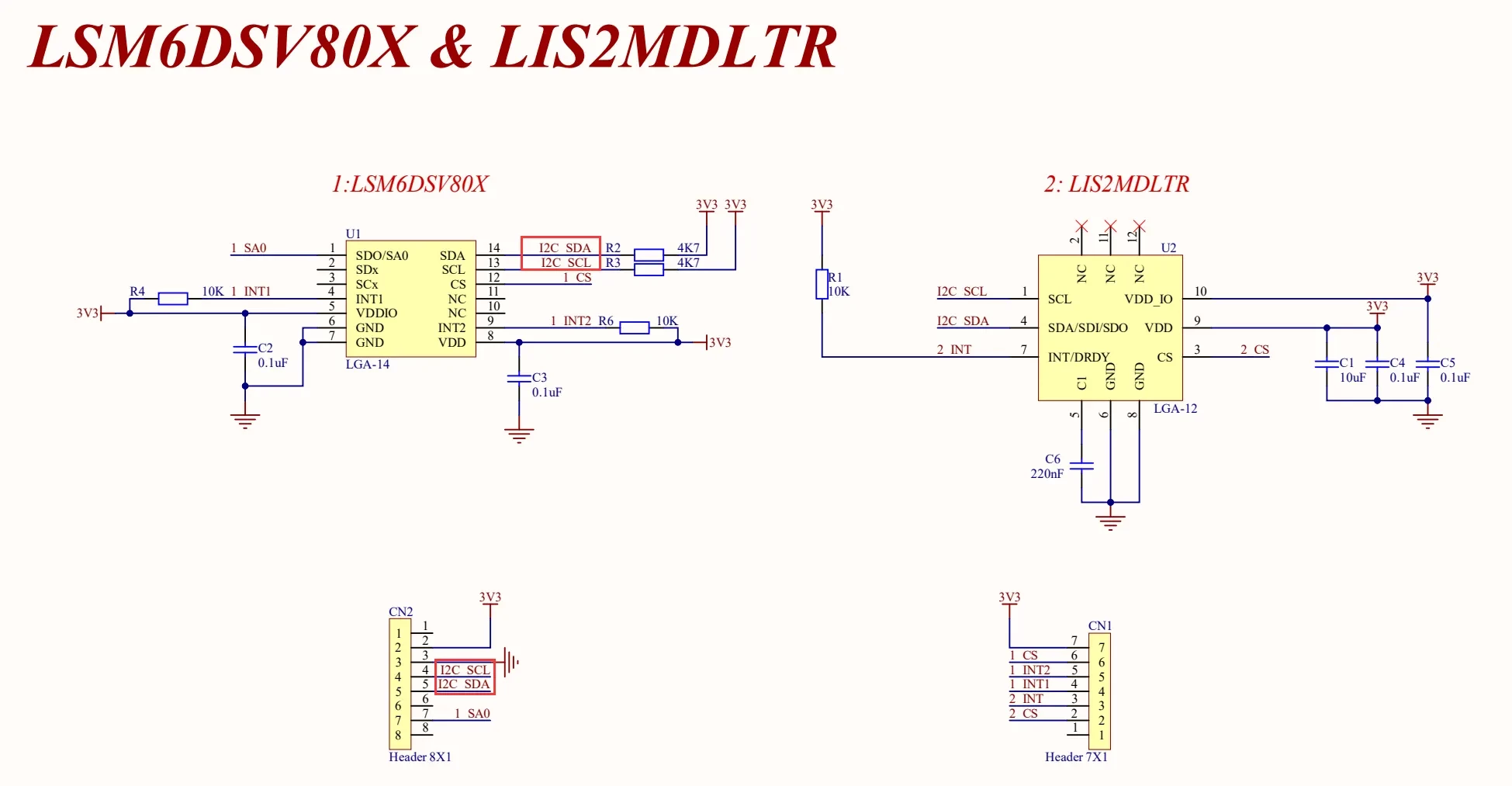
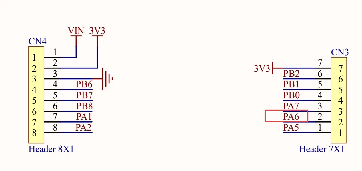
The schematic of the development board used in this article is shown below.
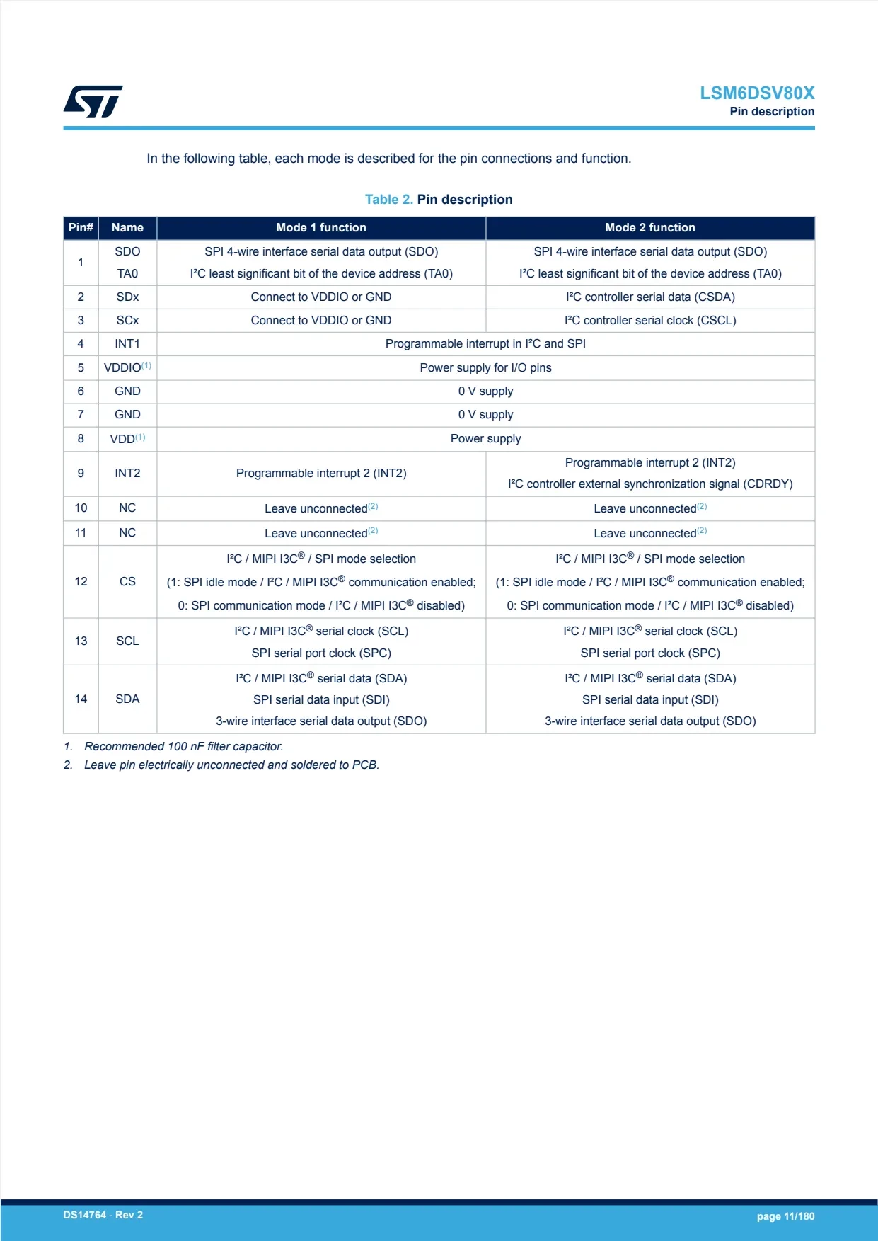
Pin Definition
I²C Communication Mode
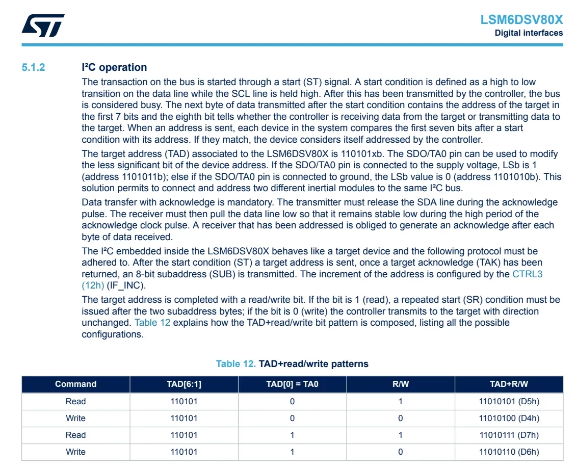
When the I²C communication interface is used, the SA0 pin determines the least significant bit of the device’s I²C address.
The device address can be configured through the SA0 pin:
-
When SA0 is connected to the supply voltage, the least significant bit is set to
1, and the 7-bit I²C address is1101011b(0x6B). -
When SA0 is connected to ground, the least significant bit is set to
0, and the 7-bit I²C address is1101010b(0x6A).
The interface is shown below.
The main pins used are CS, SCL, SDA, and SA0.
Communication Speed
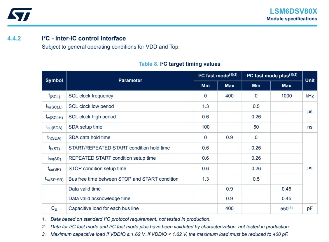
The module supports the following I²C communication speeds:
-
Standard mode: 100 kHz
-
Fast mode: 400 kHz
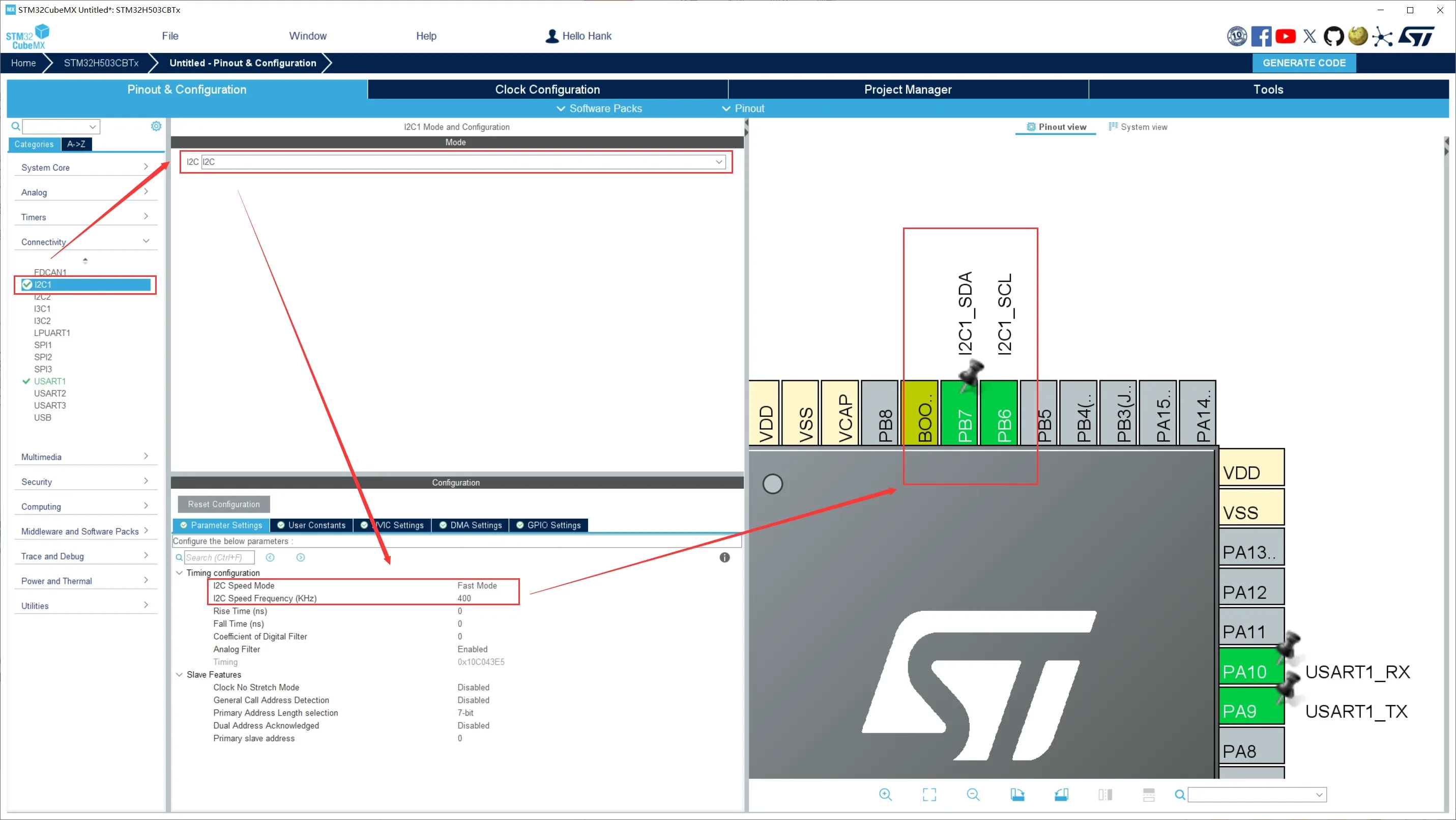
I²C Configuration
The LSM6DSV80X supports a maximum I²C communication speed of 1 MHz. In this example, the I²C bus speed is configured to 400 kHz.
CS and SA0 Configuration
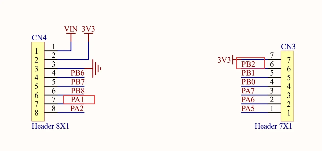
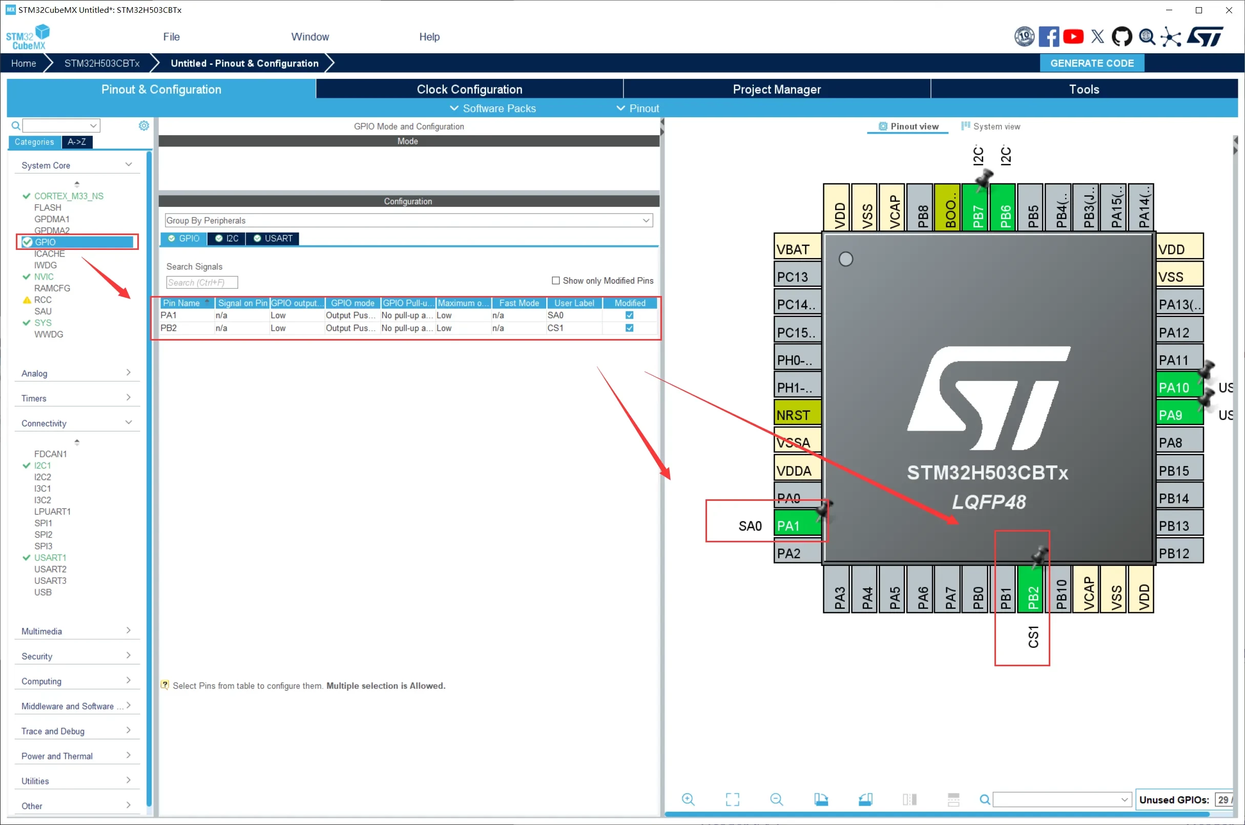
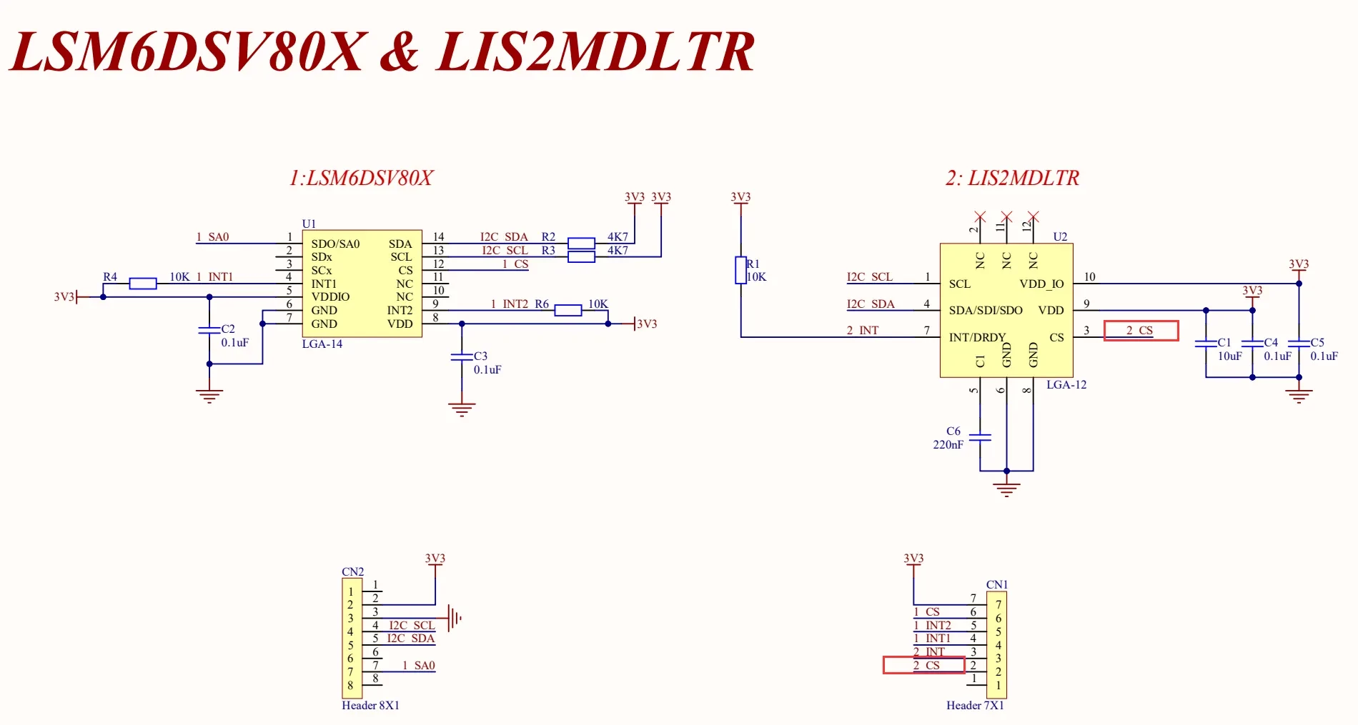
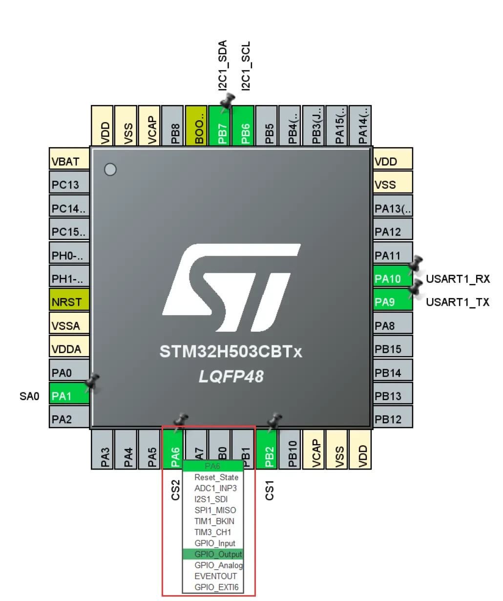
Since the board also includes a magnetometer, its CS pin must also be enabled and configured.
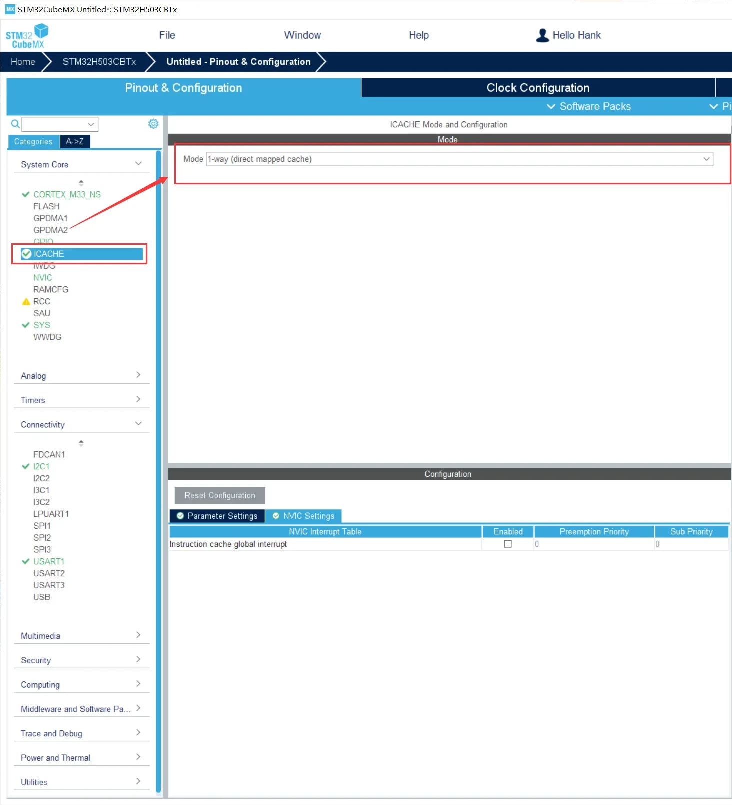
ICASHE
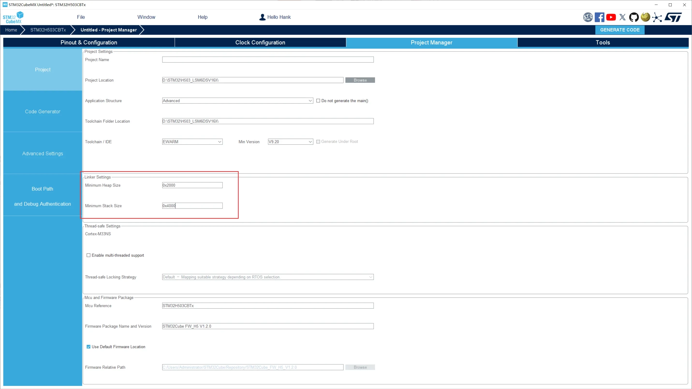
Stack Configuration
UART Retargeting
Open the Options for Target window by clicking the magic wand icon, and enable Use MicroLIB.
In main.c, add the required header file. Otherwise, the following compilation error may occur:
identifier "FILE" is undefined
/* USER CODE BEGIN Includes */
#include "stdio.h"
/* USER CODE END Includes */
Function Declaration and UART Retargeting
/* USER CODE BEGIN PFP */
int fputc(int ch, FILE *f){
	HAL_UART_Transmit(&huart1 , (uint8_t *)&ch, 1, 0xFFFF);
return ch;
}
/* USER CODE END PFP */
Reference Driver
The official LSM6DSV80X driver is available at:
https://github.com/STMicroelectronics/lsm6dsv80x-pid
Pin Initialization
Since the LSM6DSV80X_I2C_ADD_L address is used and the device operates in I²C mode, configure the relevant pins as follows:
-
Set the CS pin high to enable I²C mode.
-
Set the SA0 pin low to select the
LSM6DSV80X_I2C_ADD_Laddress.
	printf("HELLO!\n");
  HAL_GPIO_WritePin(CS1_GPIO_Port, CS1_Pin, GPIO_PIN_SET);
  HAL_GPIO_WritePin(SA0_GPIO_Port, SA0_Pin, GPIO_PIN_RESET);
  HAL_GPIO_WritePin(CS2_GPIO_Port, CS2_Pin, GPIO_PIN_SET);
	HAL_Delay(100);

	lsm6dsv80x_reset_t rst;
  stmdev_ctx_t dev_ctx;
// 累加器和计数器,用于计算均值
  double_t lowg_xl_sum[3], hg_xl_sum[3], gyro_sum[3], temp_sum;
  uint16_t lowg_xl_cnt = 0, hg_xl_cnt = 0, gyro_cnt = 0, temp_cnt = 0;

/* Initialize mems driver interface */
  dev_ctx.write_reg = platform_write;
  dev_ctx.read_reg = platform_read;
  dev_ctx.mdelay = platform_delay;
  dev_ctx.handle = &SENSOR_BUS;
/* Init test platform */
//  platform_init();
/* Wait sensor boot time */
  platform_delay(BOOT_TIME);
Reading the Device ID
Read the fixed value from the WHO_AM_I register (0x0F) and verify whether the returned value is 0x73.

Use the lsm6dsv80x_device_id_get() function to read the device ID.
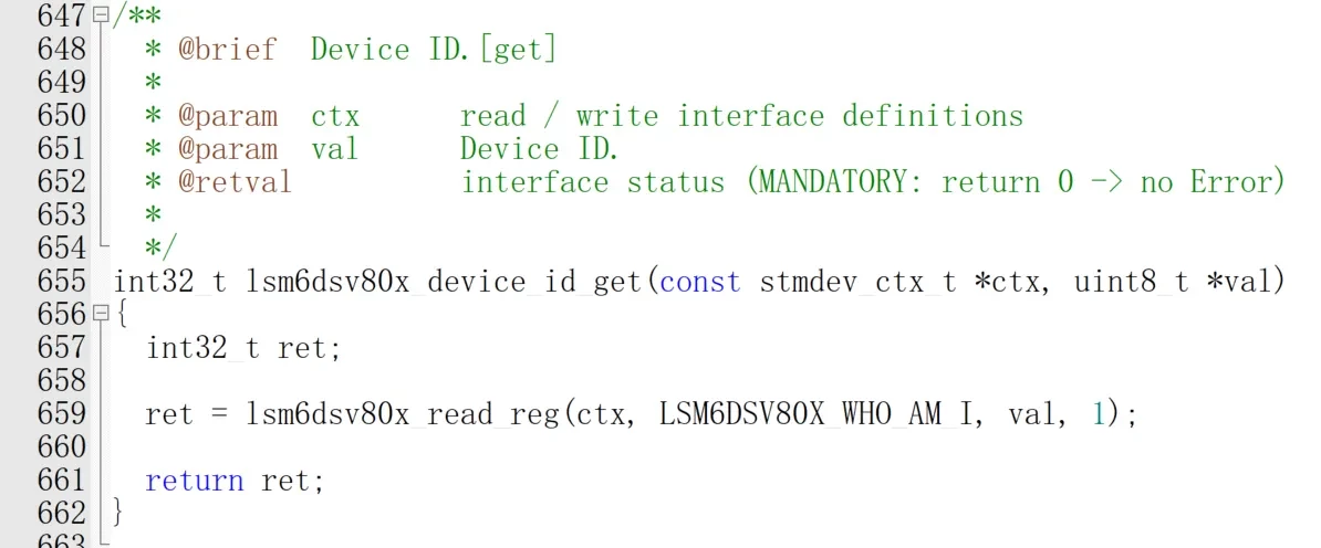
The corresponding driver code for reading the device ID is shown below.
  /* Check device ID */
  lsm6dsv80x_device_id_get(&dev_ctx, &whoamI);
printf("LSM6DSV80X_ID=0x%x,whoamI=0x%x",LSM6DSV80X_ID,whoamI);
if (whoamI != LSM6DSV80X_ID)
while (1);
Reset Operation
Reset the device by writing 1 to the SW_RESET bit in the CTRL3 register (0x12).
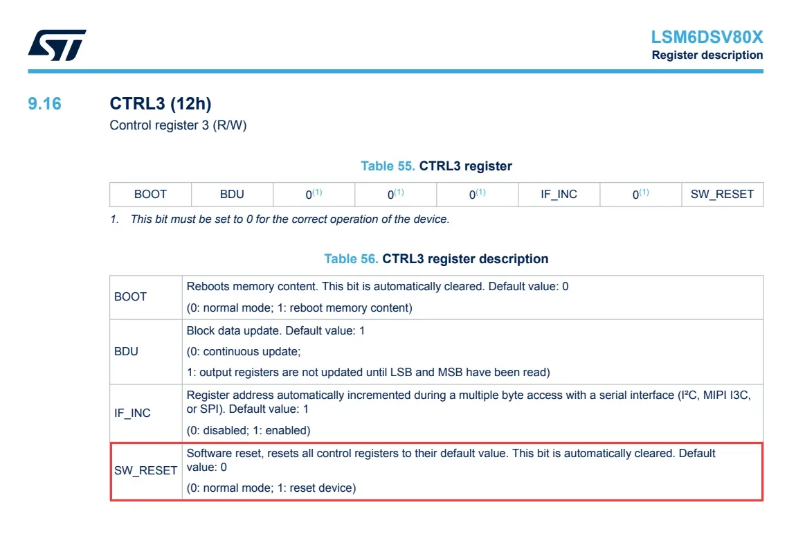
Use the lsm6dsv80x_reset_set() function to reset the device.
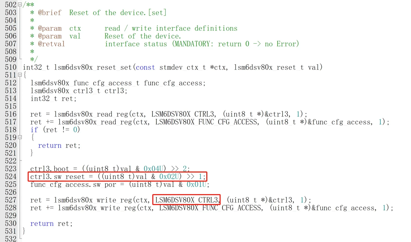
The corresponding driver code is shown below.
  /* Restore default configuration */
  lsm6dsv80x_reset_set(&dev_ctx, LSM6DSV80X_RESTORE_CTRL_REGS);
do {
    lsm6dsv80x_reset_get(&dev_ctx, &rst);
  } while (rst != LSM6DSV80X_READY);
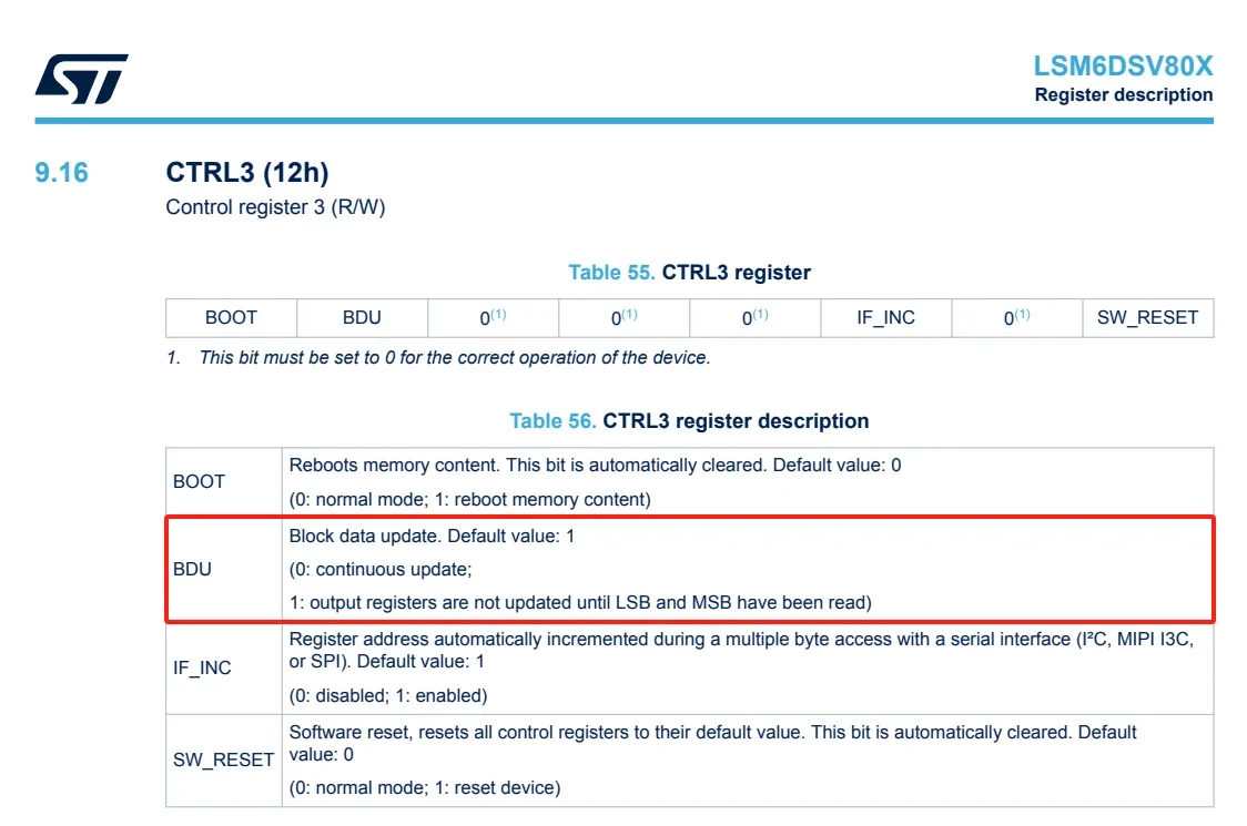
Block Data Update (BDU)
In many sensors, measurement data is stored in output registers that are divided into two parts: the Most Significant Byte (MSB) and the Least Significant Byte (LSB). These two bytes together represent a complete measurement value. For example, in an accelerometer, the MSB and LSB together represent one acceleration sample.
Continuous Update Mode (BDU = 0)
By default, the output registers are continuously updated with new measurement data. As a result, while the MCU is reading the MSB and LSB, the sensor may update the registers with a new sample.
This can lead to inconsistent data. For example, the MSB may belong to the previous sample, while the LSB belongs to the next sample. The combined result does not represent any valid measurement and may introduce errors.
Block Data Update Mode (BDU = 1)
When the BDU function is enabled, the output registers are locked during the read operation. Once the MCU starts reading either the MSB or LSB, the register contents remain unchanged until both bytes have been read.
This guarantees that the MSB and LSB belong to the same measurement sample, ensuring data consistency and preventing corrupted or mixed readings.
In short, enabling the BDU function ensures that the output registers remain stable during a read operation, preventing inconsistent data. This feature is especially important in applications requiring high accuracy and reliable measurements.
To enable BDU, write 1 to the BDU bit in the CTRL3 register (0x12).
Block Data Update (BDU)
In many sensors, measurement data is stored in output registers that are divided into two parts: the Most Significant Byte (MSB) and the Least Significant Byte (LSB). These two bytes together represent a complete measurement value. For example, in an accelerometer, the MSB and LSB together represent one acceleration sample.
Continuous Update Mode (BDU = 0)
By default, the output registers are continuously updated with new measurement data. As a result, while the MCU is reading the MSB and LSB, the sensor may update the registers with a new sample.
This can lead to inconsistent data. For example, the MSB may belong to the previous sample, while the LSB belongs to the next sample. The combined result does not represent any valid measurement and may introduce errors.
Block Data Update Mode (BDU = 1)
When the BDU function is enabled, the output registers are locked during the read operation. Once the MCU starts reading either the MSB or LSB, the register contents remain unchanged until both bytes have been read.
This guarantees that the MSB and LSB belong to the same measurement sample, ensuring data consistency and preventing corrupted or mixed readings.
In short, enabling the BDU function ensures that the output registers remain stable during a read operation, preventing inconsistent data. This feature is especially important in applications requiring high accuracy and reliable measurements.
To enable BDU, write 1 to the BDU bit in the CTRL3 register (0x12).