


jg_spitfire
Senior
May 22, 2020
Question

How to get the LSM9DS1 recommended power-up sequence?

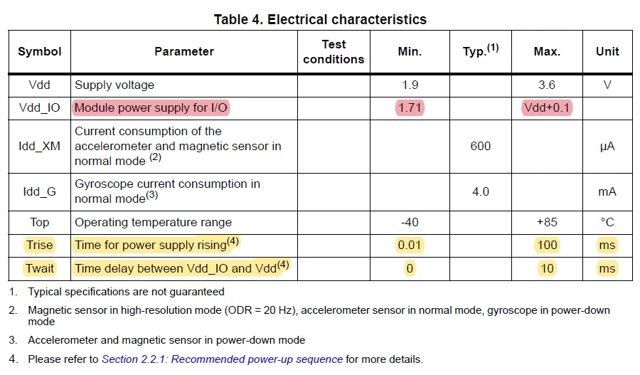
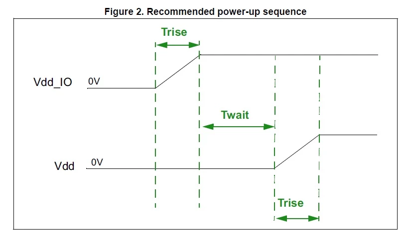
Hi, I am reading the datasheet of LSM9DS1 and it says that there are two times (rise and wait) you should respect
0693W000001chJ1QAI.jpg

0693W000001chHZQAY.jpg

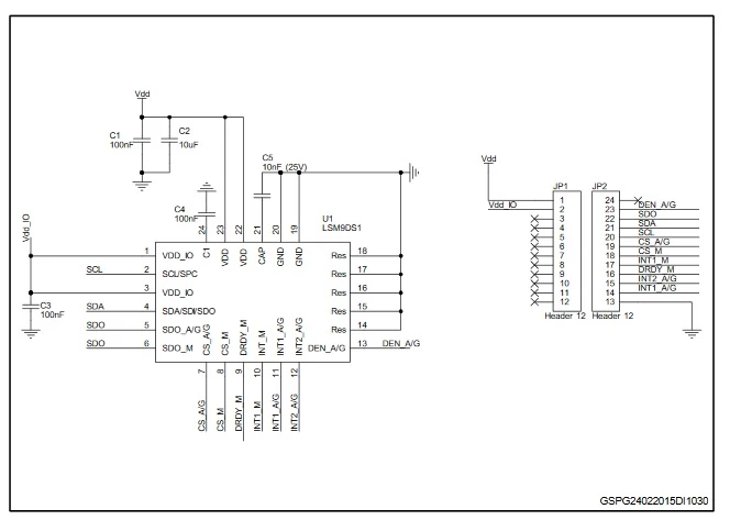
I was thinking in a sequencer IC but if we see the schematic of the LSM9DS1 evaluation board (STEVAL-MKI159V1) it does not use any kind of external IC to control the power up time, they just connects the Vdd and Vdd_IO directly to the power supply, why?, is there no consequence in supply the IMU without meet the requirements of the datasheet?, thanks
0693W000001chHyQAI.jpg

This topic has been closed for replies.

4 replies

Eleon BORLINI
ST Employee
May 22, 2020

Hi @jg_spitfire​ , considering the schematic of the STEVAL-MKI159V1 you posted above, there is no short path between Vdd and Vdd_IO: the two lines are separated and are supposed to be tied to a couple of application processor (uC) pins: this is coherent with the sequential power-on scheme of the datasheet. What I however can tell you is that 99.9% of the times you will not encounter issues in connecting together the Vdd and the Vdd_IO lines (but in this way you will maybe have a little extra current consumption in power down), provided that your Vdd / Vdd_IO ramp is not too fast (<< Trise). Regards

jg_spitfire
Senior
June 2, 2020

Hi, so I understand that I should implement the delay between the two pins, I am thinking in use a soft start LDO for each pin because with the uC I can not control the Vdd_IO rise time, what do you think?, is there any datasheet with that circuit reference? , thanks

Occio
Associate
October 20, 2021

Hi,

I followed the discussion and I'm wondering if at the end you figured out how to power up correctly the MKI159V1 module.

Thanks in any case.