
STM32 MCU datasheets: Expected preliminary updates
- October 12, 2026 at 11:17 AM
- 0 replies
- 7356 views
Introduction
This article includes preliminary updates of STM32 MCU datasheets reported since 1st January 2024. It highlights the current description requiring update and the expected one if available.
The purpose of this article is to deliver any expected updates to our MCU datasheets prior to actual documentation releases. We wish to be transparent with our updates and provide them as fast as possible, to assist you in your design process.
This article is updated on a quarterly basis. Once these preliminary updates are manifested in the datasheets, this article is refreshed with new information.
Moving forward, we are also working on providing datasheet releases on a more frequent basis.
IMPORTANT NOTICE - READ CAREFULLY :
- STMicroelectronics NV and its subsidiaries (“ST”) reserve the right to make changes, corrections, enhancements, modifications, and improvements to this article at any time without notice.
- Information in this article supersedes and replaces information previously supplied in any prior versions of this article.
- The following table gives a quick reference to the preliminary documentation updates which may be changed or improved without notice.
- This article will be reviewed on a quarterly basis and applied updates will be removed from the table.
- The hyperlinks under "Doc Reference - Revision" provides a direct link to the specific document page where the description is located.
Summary of documentation updates: "STM32 MCU datasheets"
| Function | Series (Lines) / | Update Location | Current Description / | Date |
| Description | STM32N6x5xx STM32N6x7xx DS14791 Rev 10 (Aug 2026) | Table 2. STM32N645xx features and peripheral counts Table 3. STM32N647xx features and peripheral counts Table 4. STM32N655xx features and peripheral counts Table 5. STM32N657xx features and peripheral counts | Expected: Add ETH-RMII and ETH-RGMII information in the communication interface group | Sep 2026 |
| STM32F373xx (Jun 2016) | Table 2. Device overview | Expected: Remove the following note: 1. UFBGA100 package available on 256-KB versions only The UFBGA100 package is available for 256k, 128k and 64k. STM32F373V8 - 64 Kbytes Flash, UFBGA100 STM32F373VB - 128 Kbytes Flash, UFBGA100 STM32F373VC - 256 kbytes Flash, UFBGA100 | Sep 2026 | |
| Features and peripheral counts
| STM32F765xx STM32F767xx STM32F768Ax STM32F769xx (Jul 2025) | Figure 1. Compatible board design for LQFP100 package | Current: The following sentence under Figure 1: The STM32F76x LQFP144, LQFP176, LQFP208, TFBGA216, UFBGA176 packages are fully pin-to-pin compatible with STM32F4xx devices. Expected: Update the sentence as follows: The STM32F76x and STM32F4xx devices are indeed pin-to-pin compatible when not considering packages that include the DSI peripheral. | Mar 2026 |
| STM32WBA6xxx (Jul 2025) | Table 2. Device features and peripheral counts | Current:  Expected: 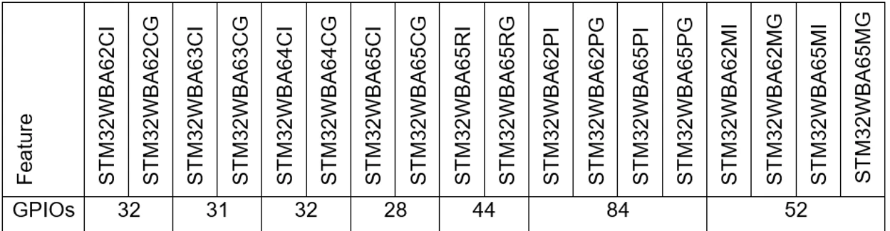
| Jun 2026
| |
| STM32WL31xx DS14836 Rev 1 (Feb 2025) | Figure 1. Block diagram | Expected: Remove the SRAM1 from Block diagram figure | Jun 2026 | |
| STM32WL5MOC (Oct 2024) | Table 1. STM32WL5MOC features and peripheral counts
| Current: For ADC (number of channels, ext + int), Expected: For ADC (number of channels, ext + int), (of which two external channels cannot be used in STM32WL5MOCH6S) | Jun 2026 | |
| Current: For GPIOs feature: 37 (35 on STM32WL5MOCH6S) Expected: For GPIOs feature: 37 (of which four GPIOs are used to control the STSAFE-A110 in STM32WL5MOCH6S) | Jun 2026 | |||
| STM32F469xx (Nov 2023) | Table 2. STM32F469xx features and peripheral counts | Current: Package for STM32F469Zx : LQPF Expected: Package for STM32F469Zx : "LQFP" | Jun 2025 | |
|
Pinouts, pin description and alternate functions
| STM32H7B0xB (May 2022) | Table 14. Port G alternate functions | Current: Alternate FMC Information is missing for PG15. Expected: Add FMC_SDNCAS alternate function for PG15. | Dec 2024 |
| STM32H7B0xB (May 2022) | Table 7. STM32H7B0xB pin/ball definition | Current: PG1 is FT_h2 Expected: PG1 must be FT_ah2 due to OPAMP2_VINM analog additional function. | Dec 2024 | |
| STM32F373xx (Jun 2016) | Table 12. Alternate functions for port PA. | Current: Missing USB mapped on PA11-PA12 as AF14 Expected: Add USB mapped on PA11-PA12 as AF14. | Apr | |
| STM32WBA6xxx (Jul 2025) | Figure 14. UFBGA121_USB ballout
Figure 15. UFBGA121_SMPS_USB ballout | Current : pin E1 named VEF+ in Figure 14. and Figure15 (page 76/77) Expected: Change VEF+ to VREF+ | Sep 2025 | |
| STM32F722xx STM32F723xx (Jul 2022) | Figure 24. STM32F723xx UFBGA176 ballout | Current: Figure name: STM32F723xx UFBGA176 ballout Expected: Figure name: STM32F722xx UFBGA176 ballout | Dec 2025 | |
| STM32F722xx STM32F723xx (Jul 2022) | Table 10. STM32F722xx and STM32F723xx pin and ball definition | Expected: Add column for the VQFPN68 package | Dec 2025 | |
| STM32U375xx (Feb 2026) | Table 20. Legend/abbreviations used in the pinout table | Expected: For I/O structure, remove _t abbreviation line | Dec 2025 | |
| STM32WL5MOC (Oct 2024) | Table 4. STM32WL5MOC pin definition | Current: For Pin number 1, the I/O structure is FT Expected: For Pin number 1, I/O structure is RST | Jun 2026 | |
| STM32H7S3x8 STM32H7S7x8 DS14359 Rev 7 (Jun 2026)
STM32H7R3x8 STM32H7R7x8 DS14360 Rev 6 (Jun 2026) | Table 21. STM32H7Sxx8 pin and ball descriptions | Current: Note 4: XSPIM_P1 I/O and XSPIM_P2 I/O are supplied respectively by VDDXSPI1 and VDDXSPI2 Expected: XSPIM_P1 I/O and XSPIM_P2 I/O are supplied respectively by VDDXSPI1 and VDDXSPI2. The EN_XSPIM1 and EN_XSPIM2 bits in PWR control register 2 (PWR_CSR2) must be set according to the selected XSPI interface. | Sep 2026 | |
| Electrical Characteristics | STM32L552xx (Oct 2020) | Table 109. ADC characteristics | Current: Missing VCMIN value. Expected: Add the VCMIN value 
| Dec 2025 |
| STM32H725xE STM32H725xG (Nov 2023) | Table 48. Flash memory programming | Current: Sector (128 Kbytes) erase time for Program/erase parallelism X 64 is missing in Table 48. Flash memory programming Expected: Add a line with this information: - Symbol : tERASE 128KB - Parameter: Sector (128 Kbytes) erase time - Conditions: Program/erase parallelism x 64 - Typ :1s - Max: 2s | Sep 2025 | |
| STM32H523xx (Nov 2024)
STM32H533xx (Nov 2024) | Table . Dynamic characteristics: eMMC characteristics, VDD = 1.71 to 1.9 V | Current: - The max value for Output valid time HS: 7/5 - Footnote (3). When using PB13 and PB14 Expected: - For Output valid time HS, replace the max value '7/5' by 7/75' - Replace the footnote (3): " When using PB13 & PB14" by "When using PB13" | Jun | |
| STM32U083xC (Mar 2024)
STM32U073x8 STM32U073xB STM32U073xC (Mar 2024)
STM32U031x4 STM32U031x6/8 (Mar 2024) | 3.4.2 Embedded SRAM | Expected: Delete the following sentence from SRAM description: It is write-protected with a 1-Kbyte granularity. | Jun 2025 | |
| STM32H747xI/G (Jan 2026) | Table 53. DSI regulator characteristics | Current: Parameter: Regulator output voltage on VDDDS Expected: Parameter: Regulator input voltage on VDDDS | Mar 2026 | |
| STM32H503xx (Oct 2024) | "12-bit ADC characteristics" section | Current: "Unless otherwise specified, the parameters given in Table xx are derived from tests performed under the ambient temperature, fPCLK2 frequency and VDDA supply voltage conditions summarized in Table yy" Expected: Replace "fPCLK2 frequency" by "fHCLK frequency" from the first paragraph in the "12-bit ADC characteristics" section. | Mar 2024 | |
| STM32H735xG (Nov 2023) | "16-bit ADC characteristics" sub sections located in sections: - Electrical characteristics (rev Y) - Electrical characteristics (rev V) sections | Current: "Unless otherwise specified, the parameters given in Table xx are derived from tests performed under the ambient temperature, fPCLK2 frequency and VDDA supply voltage conditions summarized in Table : General operating conditions". Expected: Replace "fPCLK2 frequency" by "fHCLK frequency "from the first paragraph. | Mar 2024
| |
| STM32H735xG (Nov 2023) | Table 89. 12-bit ADC accuracy | Expected: EG Typical = +/-2 LSBs EG Max = +/-5 LSBs | May 2024 | |
| STM32F479xx (Nov 2023)
STM32F469xx (Nov 2023) | “ADC characteristics” table | Current: Note 2 in the "ADC characteristics” table:
Expected: Update Note 2 to: 2. When VDDA and VREF+ are supplied by independent voltage sources, it is recommended to maintain the difference between VDDA and VREF+ below 1.8V during the power-up phase. | Jun 2025 | |
| STM32U385xx DS14830 Rev 3 (Feb 2026)
STM32U375xx (Feb 2026) | Figure xx. STM32U385xx power supply scheme (with SMPS) | Expected: Remove the following sentence (page 94), in the note of Figure 25. STM32U385xx power supply scheme (with SMPS) A 2.2 μH coil and a 2.2 μF capacitor on each VDD11 pin are then required. | Jun 2026 | |
| STM32U385xx DS14830 Rev 3 (Feb 2026)
STM32U375xx (Feb 2026) | Table xx. Flash memory characteristics | Expected: For tME, parameter: Mass erase time (two banks)
| Jun 2026 | |
| STM32U385xx DS14830 Rev 3 (Feb 2026)
STM32U375xx (Feb 2026) | Table xx. 12-bit ADC characteristics | Expected: The Max value for: fADC, ADC clock frequency: 35 fs symbol:
| Jun 2026 | |
| STM32U385xx DS14830 Rev 3 (Feb 2026)
STM32U375xx (Feb 2026) | Table xx. Maximum RAIN for 12-bit ADC | Expected: Remove the column “Sampling cycle at 55 MHz” | Jun 2026 | |
| STM32U385xx DS14830 Rev 3 (Feb 2026)
STM32U375xx (Feb 2026) | Table 97. 12-bit ADC accuracy | Current:
Expected:
| Jun 2026 | |
| STM32H757xI (Jan 2026)
STM32H742xI/G STM32H743xI/G (Jan 2026)
STM32H753xI (Jan 2026) STM32H750VB STM32H750ZB STM32H750IB STM32H750XB (Jan 2026)
STM32H755xI (Jan 2026)
STM32H745xI/G (Jan 2026)
STM32H747xI/G (Jan 2026)
STM32H757xI (Jan 2026) | PLL characteristics | Expected: Replace VDDA by VDD in all “PLL characteristics” Tables. | Jun 2026 | |
| STM32N6x5xx STM32N6x7xx (Dec 2025) | Table 88. XSPI characteristics in DTR mode without DQS | Expected: Add the following note in the tw(CS) row, for the value 3xt(CLK) Note: XSPI_DCR1_CSHT[5:0] = 0x1 | Jun 2026 | |
| STM32H7S3x8 STM32H7S7x8 DS14359 Rev 7 (Jun 2026) STM32H7R3x8 STM32H7R7x8 DS14360 Rev 6 (Jun 2026) | Table x. General operating conditions | Expected: Update the line relative to fcpu and delete note 9
| Sep 2026 | |
| STM32H7S3x8 STM32H7S7x8 DS14359 Rev 7 (Jun 2026)
STM32H7R3x8 STM32H7R7x8 DS14360 Rev 6 (Jun 2026) | EXTI section | Expected: Add the following section EXTI in section 6.3, after sub section “6.3.16 NRST pin characteristics”
| Sep 2026 | |
| STM32C071x8 STM32C071xB (Apr 2025)
STM32C091xB STM32C091xC STM32C092xB STM32C092xC (Mar 2026) | Table 28. Current consumption in Run mode from flash memory at different die temperatures | Expected: IDD(Run) 32.768 kHz for Supply current in Run mode 25°C Max = 0.120mA | Sep 2026 | |
| STM32N6x5xx STM32N6x7xx DS14791 Rev 10 (Aug 2026) | Table 120. Dynamic characteristics: Ethernet MAC signals for MDIO/SMA | Expected: Add the following information: Ethernet Primary interface GPIOs with advanced feature enabled configuration
| Sep 2026 | |
| STM32N6x5xx STM32N6x7xx DS14791 Rev 10 (Aug 2026) | Features | Current: In the section graphics (page 1) • LCD-TFT controller up to XGA resolution Expected: • LCD-TFT controller up to 720p30, 24 bpp | Sep 2026 | |
| STM32F405xx STM32F407xx DS8626 Rev 12 (Mar 2026) | Table 67. ADC characteristics | Current: Note 2: It is recommended to maintain the voltage difference between VREF+ and VDDA below 1.8 V. Expected: 2. When VDDA and VREF+ are supplied by independent voltage sources, during power-up phase, it is recommended to maintain the difference between VDDA and VREF+ below 1.8V. | Sep 2026 | |
| STM32N6x5xx STM32N6x7xx DS14791 Rev 10 (Aug 2026) | Table 86. FMC SDRAM read timings | Expected: Add the following information, above Table 86. FMC SDRAM read timings:
| Sep 2026 | |
| STM32N6x5xx STM32N6x7xx DS14791 Rev 10 (Aug 2026) | 108. DCMIPP characteristics | Add the following information, above Table 108. DCMIPP characteristics DCMIPP Primary interface GPIOs with advanced feature enabled configuration
GPIOB->ADVCFGRL=0xCC000000; GPIOB->ADVCFGRH=0x0C0000CC;
GPIOD->ADVCFGRL=0xC0CCC00C; GPIOD->ADVCFGRH=0x00CCC00C;
GPIOE->ADVCFGRL=0x0CC000CC; GPIOE->ADVCFGRH=0x0000000C; | Sep 2026 | |
| STM32N6x5xx STM32N6x7xx DS14791 Rev 10 (Aug 2026) | Table 111. LCD-TFT characteristics:
| Add the following information, above Table 111. LCD-TFT characteristics: LTDC Primary interface GPIOs with advanced feature enabled and peripheral configurations
LTDC_CLK (PA5) clock polarity retime configuration
LTDC_GCR->PCPOL=0x0 | Sep 2026 | |
| Functional overview
| STM32WBA6xxx (Jul 2025) | Figure 6. Clock tree | Expected: Update UARTx to USARTx in Clock tree Figure | Sep 2025 |
| STM32H747xI/G (Jan 2026) | 3.5.1 Power supply scheme | Current: - VDDDSI = 1.62 to 3.6 V: supply voltage for the DSI internal regulator - VDD12DSI = 1.15 to 1.3 V: optional supply voltage for the DSI PHY (DSI regulator off) - VCAPDSI: DSI regulator supply output Expected: - VDDDSI=1.62 to 3.6 V: supply voltage for the DSI internal regulator. If VDDDSI is not available, it is connected internally to VDD. - VDD12DSI=1.15 to 1.3 V: DSI PHY supply input - VCAPDSI: DSI regulator supply output. It must be connected to VDD12DSI if VDD12DSI pin is available; otherwise, it is connected internally to VCAPDSI. | Mar 2026 | |
| STM32H725xE/G (Nov 2023) | Table x. Timer feature comparison
| Current: The maximum timer clock is up to 550 MHz depending on the TIMPRE bit in the RCC_CFGR register and D2PRE1/2 bits in Expected: The maximum timer clock is up to 275 MHz depending on the TIMPRE bit in the RCC_CFGR register and D2PRE1/2 bits in RCC_D2CFGR register. | Mar 2025 | |
| STM32H735xG (Nov 2023) | ||||
| STM32H733VG STM32H733ZG (Nov 2023) | ||||
| STM32U083xC (Mar 2024)
STM32U073xx (Mar 2024) | Table 40. Current consumption in Stop 2 mode | Current: For “LCD disabled” condition: - EN_ULP = 0 - EN_ULP = 1 Expected: For “LCD disabled” condition: - EN_ULP = 1 - EN_ULP = 0 | Jun 2024 | |
| Table 41. Current consumption in Standby mode | Current: For “No independent watchdog” condition: - EN_ULP = 0 - EN_ULP = 1 Expected: For “No independent watchdog” condition: - EN_ULP = 1 - EN_ULP = 0 | Jun 2024 | ||
| Table 42. Current consumption in Shutdown mode | Expected: Remove in Conditions column: EN_ULP=0 | Jun 2024 | ||
| STM32H503xx (Oct 2024) | Table 33. Peripheral current consumption in Sleep mode | Current: Table name: “Table 33. Peripheral current consumption in sleep mode” Expected: Change the name of the table to “Table 33. Peripheral current consumption” | Jun 2025 | |
| STM32H735xG (Nov 2023) | Table 31. "Typical and maximum current consumption in Standby mode" | Current: The max values are present for “RTC and LSE” ON Expected: The max values for “RTC and LSE” should be placed for “RTC and LSE” OFF | Aug 2024 | |
| STM32L4A6xG (Jul 2022)
Applicable for ALL STM32L4 | 3.29.2 General-purpose timers (TIM2, TIM3, TIM4, TIM5, TIM15, TIM16, TIM17) | Current: TIM2 has a 32-bit auto-reload up/downcounter and 32-bit prescaler. Expected: TIM2 has a 32-bit auto-reload up/downcounter and 16-bit prescaler | Jun 2026 | |
| STM32H503xx (Oct 2024) | 3.29 Controller area network (FDCAN) | Expected: Add the following note at the end of the section: Note: The WLCSP25 and UFQFPN32 devices do not support the HSE. When using FDCAN, the HSI can be used as the clock source via the PLL to drive the FDCAN. It is recommended to perform clock calibration to ensure the FDCAN clock source frequency remains within ±1.5%. For more details, please refer to AN6202, "How to Calibrate Internal RC Oscillators on STM32H5 MCUs.” | Jun 2026 | |
| STM32WBA5xxx (May 2026) | 3.7 Boot modes | Current: The bootloader is located in the system memory, programmed by ST during production. It is used to program the flash memory by using USART, I2C or SPI in device mode. Expected: Add text: "Availability of interfaces depend on package pinout and device supported peripherals." | Jun 2026 | |
| STM32WBA6xxx (Jul 2025) | 3.12.2 Power supply supervisor | In section “Standby mode”: Current: The IWDG can remain active in Standby mode. Expected: The IWDG, RTC, and TAMP can remain active in Standby mode. | Jun 2026 | |
| STM32WBA6xxx (Jul 2025) | 3.14.1 GPIO using PD6 and PD7 | Expected: Remove this section “3.14.1 GPIO using PD6 and PD7” | Jun 2026 | |
| STM32H5Exxx (Feb 2026) | 3.42.2 General-purpose timers (TIM2, TIM3, TIM4, TIM5, TIM15, TIM16, TIM17) | Current: Title: General-purpose timers (TIM2, TIM3, TIM4, TIM5, TIM15, TIM16, TIM17) Expected: General-purpose timers (TIM2, TIM3, TIM4, TIM5, TIM12, TIM13, TIM14, TIM15, TIM16, TIM17) | Jun 2026 | |
| STM32U385xx DS14830 Rev 3 (Feb 2026)
STM32U375xx (Feb 2026)
| 3.11 Reset and clock controller (RCC) | Current: the MSI frequency can be automatically trimmed by hardware to reach better accuracy. Expected: the MSI frequency can be automatically trimmed by hardware to reach better than ±0.25% accuracy. | Jun 2026 | |
| STM32WBA2xxx (May 2026) | 3.7 Boot modes | Expected: In paragraph: The bootloader is located in the system memory, programmed by ST during production. It is used to program the flash memory by using USART, I2C, SPI, or USB in device mode through the DFU (device firmware upgrade). Add the following text: "Availability of interfaces depend on package pinout and device supported peripherals." | Jun 2026 | |
| STM32L073x8 STM32L073xB STM32L073xZ (Sep 2022) | 3.17 Timers and watchdogs | Current : The ultra-low-power STM32L073xx devices include three general-purpose timers, one low-power timer (LPTIM), one basic timer, two watchdog timers and the SysTick timer. Expected : The ultra-low-power STM32L073xx devices include four general-purpose timers, one low-power timer (LPTIM), two basic timers, two watchdog timers, and the SysTick timer. Table 10 compares the features of the general-purpose and basic timers. - Update Table 10 "Timer feature comparison" to include an additional "Timer type" column: TIM2,TIM3 are general purpose timer TIM21,TIM22 are general purpose timer TIM6,TIM7 are basic timer | Sep 2026 | |
| STM32G491xC STM32G491xE (Apr 2024) | 3.5 Embedded SRAM | Current : 16 Kbytes mapped at address 0x20001 4000 (SRAM2). Expected: 16 Kbytes mapped at address 0x2001 4000 (SRAM2). | Sep 2026 | |
| Package information | STM32F722xx STM32F723xx (Jul 2022) | Table 125. Package thermal characteristics | Expected: Add this parameter: Thermal resistance junction-ambient VFQFPN68 – 8 x 8 mm / 0.5 mm pitch Value: 24.6 | Mar 2026 |
| STM32G491xC STM32G491xE (Apr 2024) | Table 100. Package thermal characteristics | Current : For ΘJC, Thermal resistance junction-ambient UFBGA64 - 5 × 5 mm = 56.1 Expected: For ΘJC, Thermal resistance junction-ambient UFBGA64 - 5 × 5 mm = 11.6 | Sep 2026 | |
| STM32F412xE STM32F412xG DS11139 Rev 9 (Jan 2024) | 7.2 WLCSP64 package information (A04F) | Current : This WLCSP is a 64-ball, 3.658 x 3.658 mm, 0.4 mm pitch wafer level chip scale. Expected This WLCSP is a 64-ball, 3.623 x 3.651 mm, 0.4 mm pitch wafer level chip scale. | Sep 2026 | |
| Application block diagrams | STM32F413xG STM32F413xH (Jan 2025) | Figure 78. Sensor Hub application example | Current: Figure 78 indicate that SWDIO is on pin PC13 Expected: Figure 78 should indicate that SWDIO is on pin PA13 | Sep 2025 |
| Datasheet | STM32WL31xx DS14836 Rev 1 (Feb 2025) | Datasheet Title | Current: The title: “Multiprotocol LPWAN 32-bit MCU Arm® Cortex®-M0+ 2(G)FSK, 4(G)FSK, ASK, D-BPSK, up to 128KB flash, 32KB SRAM” Expected: Multiprotocol LPWAN 32-bit MCU Arm® Cortex®-M0+ 2(G)FSK, 4(G)FSK, ASK, D-BPSK, up to 128KB flash, 16KB SRAM | Jun 2026 |
| Features | STM32H5Fxxx (Feb 2026) | General-purpose inputs/outputs | Current: Up to ten I/Os with independent supply down to 1.08 V Expected: Up to sixteen I/Os with independent supply down to 1.08 V | Jun 2026 |
