- STMicroelectronics Community
- STM32 MCUs
- STM32 MCUs TouchGFX and GUI
- STM32H743II: Configure SDRAM
- Subscribe to RSS Feed
- Mark Topic as New
- Mark Topic as Read
- Float this Topic for Current User
- Bookmark
- Subscribe
- Mute
- Printer Friendly Page
STM32H743II: Configure SDRAM
- Mark as New
- Bookmark
- Subscribe
- Mute
- Subscribe to RSS Feed
- Permalink
- Email to a Friend
- Report Inappropriate Content
2021-03-15 06:50 PM
For around the last month and a half I've been working on implementing the LVGL open source GUI framework on an STM32H743II utilizing this external SDRAM on a Alientek board that shares similarities to the STM32H743II-Eval board.
This should be the RAM Chip: https://www.digikey.com/en/products/detail/winbond-electronics/W9825G6KH-6/5001919
I've been able to get LVGL running and implemented along with displaying on an LTDC display I have configured properly the only hold up is that I cannot create a display buffer large enough to actually display across the entire screen so I obviously need to use the external ram to handle this.
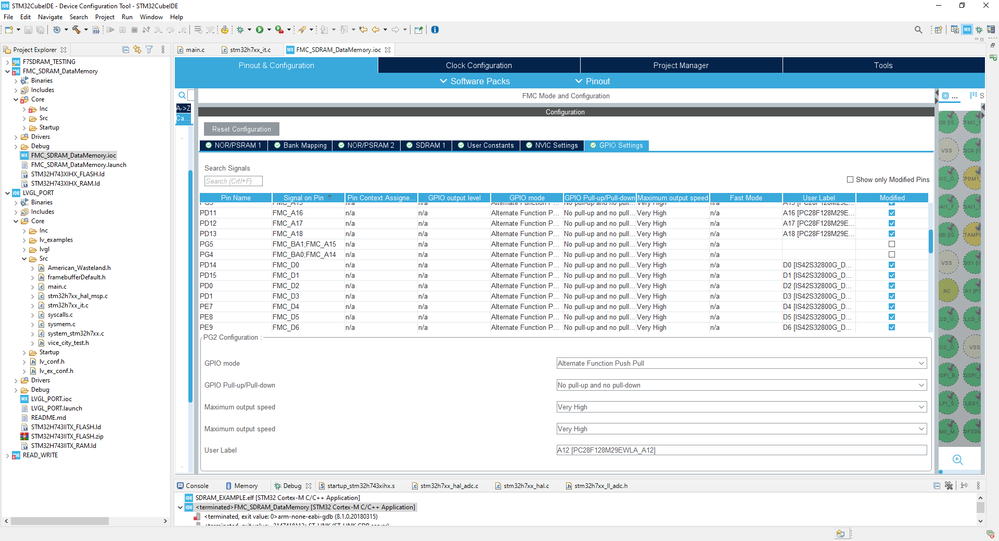
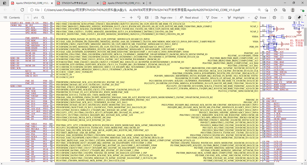
Going through the documentation provided with the board the pinout for the SDRAM appears to be the same as that generated by the CUBEMX for the STM32H743I-EVAL Board, now its possible I've misunderstood the documentation provided so I've included a couple screen shots just so people can point out if I'm clearly being stupid in terms of my physical hardware connections. 
I've attempted to implement this example: https://github.com/STMicroelectronics/STM32CubeH7/tree/master/Projects/STM32H743I-EVAL/Examples/FMC/FMC_SDRAM_DataMemory by creating a new project using the STM32H743II-Eval board template provided by the CubeIDE and copying the main.c file code over but to no avail.
Attempts to just import that example have always lead to major driver conflicts and an inability to compile so if anyone knows a good method of simply compiling that example on a fresh project that would also probably resolve my problems.
- Labels:
-
FMC-FSMC
-
LCD-LTDC
-
STM32CubeMX
-
STM32H7 Series
- Mark as New
- Bookmark
- Subscribe
- Mute
- Subscribe to RSS Feed
- Permalink
- Email to a Friend
- Report Inappropriate Content
2021-03-15 06:51 PM
MAIN Loop
int main(void)
{
  /* USER CODE BEGIN 1 */
	  /* Enable the CPU Cache */
	  CPU_CACHE_Enable();
  /* USER CODE END 1 */

  /* MCU Configuration--------------------------------------------------------*/

  /* Reset of all peripherals, Initializes the Flash interface and the Systick. */
  HAL_Init();

  /* USER CODE BEGIN Init */

  /* USER CODE END Init */

  /* Configure the system clock */
  SystemClock_Config();

  /* USER CODE BEGIN SysInit */

  /* USER CODE END SysInit */

  /* Initialize all configured peripherals */
  MX_GPIO_Init();
  MX_ADC1_Init();
  MX_DFSDM1_Init();
  MX_ETH_Init();
  MX_FMC_Init();
  MX_I2C1_Init();
  //MX_LTDC_Init();
  MX_QUADSPI_Init();
  MX_SAI1_Init();
  //MX_SDMMC1_SD_Init();
  //MX_USART1_UART_Init();
  //MX_USB_OTG_FS_PCD_Init();
  //MX_USB_OTG_HS_PCD_Init();
  /* USER CODE BEGIN 2 */


  Fill_Buffer(aTable, 1024, 0);

  /*##-2- Read address of the buffer and stack pointer address ########################*/
  uwTabAddr = (uint32_t)aTable; /* should be above 0xD0000000 */

  /* Get main stack pointer value */
  MSPValue = __get_MSP(); /* should be above 0xD0000000 */
  /* USER CODE END 2 */

  /* Infinite loop */
  /* USER CODE BEGIN WHILE */
  while (1)
  {
    /* USER CODE END WHILE */

    /* USER CODE BEGIN 3 */
  }
  /* USER CODE END 3 */
}- Mark as New
- Bookmark
- Subscribe
- Mute
- Subscribe to RSS Feed
- Permalink
- Email to a Friend
- Report Inappropriate Content
2021-03-15 06:52 PM
static void MX_FMC_Init(void)
{

  /* USER CODE BEGIN FMC_Init 0 */

  /* USER CODE END FMC_Init 0 */

  FMC_NORSRAM_TimingTypeDef Timing = {0};
  FMC_SDRAM_TimingTypeDef SdramTiming = {0};

  /* USER CODE BEGIN FMC_Init 1 */

  /* USER CODE END FMC_Init 1 */

  /** Perform the NOR1 memory initialization sequence
  */
  hnor1.Instance = FMC_NORSRAM_DEVICE;
  hnor1.Extended = FMC_NORSRAM_EXTENDED_DEVICE;
  /* hnor1.Init */
  hnor1.Init.NSBank = FMC_NORSRAM_BANK1;
  hnor1.Init.DataAddressMux = FMC_DATA_ADDRESS_MUX_DISABLE;
  hnor1.Init.MemoryType = FMC_MEMORY_TYPE_NOR;
  hnor1.Init.MemoryDataWidth = FMC_NORSRAM_MEM_BUS_WIDTH_16;
  hnor1.Init.BurstAccessMode = FMC_BURST_ACCESS_MODE_DISABLE;
  hnor1.Init.WaitSignalPolarity = FMC_WAIT_SIGNAL_POLARITY_LOW;
  hnor1.Init.WaitSignalActive = FMC_WAIT_TIMING_BEFORE_WS;
  hnor1.Init.WriteOperation = FMC_WRITE_OPERATION_DISABLE;
  hnor1.Init.WaitSignal = FMC_WAIT_SIGNAL_DISABLE;
  hnor1.Init.ExtendedMode = FMC_EXTENDED_MODE_DISABLE;
  hnor1.Init.AsynchronousWait = FMC_ASYNCHRONOUS_WAIT_ENABLE;
  hnor1.Init.WriteBurst = FMC_WRITE_BURST_DISABLE;
  hnor1.Init.ContinuousClock = FMC_CONTINUOUS_CLOCK_SYNC_ONLY;
  hnor1.Init.WriteFifo = FMC_WRITE_FIFO_ENABLE;
  hnor1.Init.PageSize = FMC_PAGE_SIZE_NONE;
  /* Timing */
  Timing.AddressSetupTime = 15;
  Timing.AddressHoldTime = 15;
  Timing.DataSetupTime = 255;
  Timing.BusTurnAroundDuration = 15;
  Timing.CLKDivision = 16;
  Timing.DataLatency = 17;
  Timing.AccessMode = FMC_ACCESS_MODE_A;
  /* ExtTiming */

  if (HAL_NOR_Init(&hnor1, &Timing, NULL) != HAL_OK)
  {
    Error_Handler( );
  }

  /** Perform the SRAM2 memory initialization sequence
  */
  hsram2.Instance = FMC_NORSRAM_DEVICE;
  hsram2.Extended = FMC_NORSRAM_EXTENDED_DEVICE;
  /* hsram2.Init */
  hsram2.Init.NSBank = FMC_NORSRAM_BANK3;
  hsram2.Init.DataAddressMux = FMC_DATA_ADDRESS_MUX_DISABLE;
  hsram2.Init.MemoryType = FMC_MEMORY_TYPE_SRAM;
  hsram2.Init.MemoryDataWidth = FMC_NORSRAM_MEM_BUS_WIDTH_16;
  hsram2.Init.BurstAccessMode = FMC_BURST_ACCESS_MODE_DISABLE;
  hsram2.Init.WaitSignalPolarity = FMC_WAIT_SIGNAL_POLARITY_LOW;
  hsram2.Init.WaitSignalActive = FMC_WAIT_TIMING_BEFORE_WS;
  hsram2.Init.WriteOperation = FMC_WRITE_OPERATION_DISABLE;
  hsram2.Init.WaitSignal = FMC_WAIT_SIGNAL_DISABLE;
  hsram2.Init.ExtendedMode = FMC_EXTENDED_MODE_DISABLE;
  hsram2.Init.AsynchronousWait = FMC_ASYNCHRONOUS_WAIT_ENABLE;
  hsram2.Init.WriteBurst = FMC_WRITE_BURST_DISABLE;
  hsram2.Init.ContinuousClock = FMC_CONTINUOUS_CLOCK_SYNC_ONLY;
  hsram2.Init.WriteFifo = FMC_WRITE_FIFO_ENABLE;
  hsram2.Init.PageSize = FMC_PAGE_SIZE_NONE;
  /* Timing */
  Timing.AddressSetupTime = 15;
  Timing.AddressHoldTime = 15;
  Timing.DataSetupTime = 255;
  Timing.BusTurnAroundDuration = 15;
  Timing.CLKDivision = 16;
  Timing.DataLatency = 17;
  Timing.AccessMode = FMC_ACCESS_MODE_A;
  /* ExtTiming */

  if (HAL_SRAM_Init(&hsram2, &Timing, NULL) != HAL_OK)
  {
    Error_Handler( );
  }

  /** Perform the SDRAM1 memory initialization sequence
  */
  hsdram1.Instance = FMC_SDRAM_DEVICE;
  /* hsdram1.Init */
  hsdram1.Init.SDBank = FMC_SDRAM_BANK2;
  hsdram1.Init.ColumnBitsNumber = FMC_SDRAM_COLUMN_BITS_NUM_8;
  hsdram1.Init.RowBitsNumber = FMC_SDRAM_ROW_BITS_NUM_11;
  hsdram1.Init.MemoryDataWidth = FMC_SDRAM_MEM_BUS_WIDTH_32;
  hsdram1.Init.InternalBankNumber = FMC_SDRAM_INTERN_BANKS_NUM_4;
  hsdram1.Init.CASLatency = FMC_SDRAM_CAS_LATENCY_1;
  hsdram1.Init.WriteProtection = FMC_SDRAM_WRITE_PROTECTION_DISABLE;
  hsdram1.Init.SDClockPeriod = FMC_SDRAM_CLOCK_DISABLE;
  hsdram1.Init.ReadBurst = FMC_SDRAM_RBURST_DISABLE;
  hsdram1.Init.ReadPipeDelay = FMC_SDRAM_RPIPE_DELAY_0;
  /* SdramTiming */
  SdramTiming.LoadToActiveDelay = 16;
  SdramTiming.ExitSelfRefreshDelay = 16;
  SdramTiming.SelfRefreshTime = 16;
  SdramTiming.RowCycleDelay = 16;
  SdramTiming.WriteRecoveryTime = 16;
  SdramTiming.RPDelay = 16;
  SdramTiming.RCDDelay = 16;

  if (HAL_SDRAM_Init(&hsdram1, &SdramTiming) != HAL_OK)
  {
    Error_Handler( );
  }

  /* USER CODE BEGIN FMC_Init 2 */

  /* USER CODE END FMC_Init 2 */
}- Screen flickering while using TFT-LCD with LTDC in STM32 MCUs products
- SDRAM with just one Bank Address pin in STM32 MCUs products
- Trouble with SDRAM and STM32F469 in STM32 MCUs products
- Error while configuring STM32H747BIT6 with SDRAM IS42S16320D(SDRAM IC). in STM32 MCUs products
- How to use external SDRAM as an data memory? in STM32 MCUs Embedded software
