- STMicroelectronics Community
- STM32 MCUs
- STM32 MCUs Wireless
- Antenna matching for chip antenna after RF switch....
- Subscribe to RSS Feed
- Mark Topic as New
- Mark Topic as Read
- Float this Topic for Current User
- Bookmark
- Subscribe
- Mute
- Printer Friendly Page
Antenna matching for chip antenna after RF switch. How to proceed?
- Mark as New
- Bookmark
- Subscribe
- Mute
- Subscribe to RSS Feed
- Permalink
- Email to a Friend
- Report Inappropriate Content
2021-02-17 09:49 PM
I'm using the same network style as the NUCLEO-WL55JC which is tuned to a different frequency. This includes the use of the BGS13S4N9 RF switch that selects Tx (HP), Tx (LP) or Rx to connect with the antenna.
The matching network design guide (AN5457) covers everything up to the switch but there's a network for matching to a connector or PCB antenna which comes after the switch.
I want to use the Johanson 0915AT43A0026 chip antenna. In the datasheet they state that a pi-type L-L-C network (4.7nH, 10nH, 0.5pF) is required for this chip with a 50Ω feed.
Some similar cases can be found on the web where a combination of both matching networks was the solution but these did not involve a switch so the "MCU" matching circuit was equivalent to what we have before the RF switch (which needs to be kept as-is).
How can the chip antenna be used with the antenna-side terminal of the 3-way RF switch?
Note: I get the impression that the existing (pcb/connector) matching is intended for a naked trace/wire antenna, which would have impedance different than 50/0 (probably around 30) but have no evidence.
- Labels:
-
STM32WL Series
- Mark as New
- Bookmark
- Subscribe
- Mute
- Subscribe to RSS Feed
- Permalink
- Email to a Friend
- Report Inappropriate Content
2021-03-03 07:14 AM
Hello @David Orr,
You can use it. There is no problem. The RF switch should see 50 Ω from your L-L-C network and your antenna chip should see its impedance conjugated.
Note that the 50 Ω feed comes from the RF SW output (when using RFO_LP or HP).
FYI: when using the RFO_HP, due to the RF power, the Pi-structure before the antenna should be used also as a low-pass filter.
Some amount of harmonic energy will pass the RF SW and reach the antenna.
In your case, your L-L-C network will acts as a LP filter.
I suggest you to simulate (AC analysis up-to 10 GHz, e.g. with LTspice) this network with the impedance of your antenna and see the attenuation inserted by this structure for the harmonic frequencies (2f0, 3f0, 4f0 etc).
FYI: the coating (solder mask layer) should not impact the impedance for such frequency range. For RF PCB, normally this layer has a thickness between 7 to 30 µm over traces. The effects of the solder mask becomes more evident for higher frequencies.
To illustrate that I performed a simulation using ADS of the characteristic impedance for a GCPW sweeping the Er and thickness of the solder mask varying the frequency from 0.1 to 10 GHz. See the PDF attached for the results.
Let me know if that answers your question.
Kind regards,
Hamilton
- Mark as New
- Bookmark
- Subscribe
- Mute
- Subscribe to RSS Feed
- Permalink
- Email to a Friend
- Report Inappropriate Content
2021-03-03 05:53 PM
Hi @Hamilton DC ,
Thanks for your help, I had been very curious about the solder mask Er effect on the antenna but had no way of checking and nothing definitive came up when searching.
I eventually found an S-parameter file from Johanson for the chip plus matching circuit.
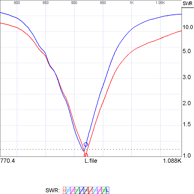
I have tuned the matching circuit from the RF design guide using SimSmith and the S-parameter file as the load.
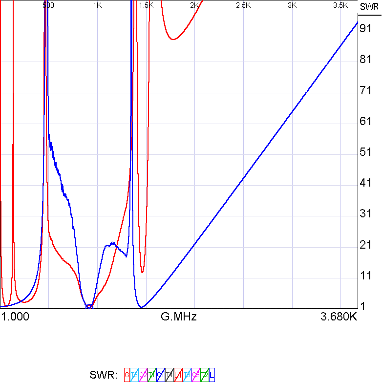
The S-parameter file doesn't reach up to harmonics of 920MHz but normal sweep does include the file data points when the range is larger.
The first image is a sweep up to 4th harmonic, blue is the S-parameter file (load) and red is with my matching circuit. You can see the discontinuity in the blue line at around 1.3GHz where the S-parameter file ends.


Does this seem reasonable to you?
- Mark as New
- Bookmark
- Subscribe
- Mute
- Subscribe to RSS Feed
- Permalink
- Email to a Friend
- Report Inappropriate Content
2021-03-04 08:16 AM
Hi @David Orr,
I'm trying a few things to show you.
Can you post the S-parameters file, please?
I'm not finding the antenna's output impedance, or otherwise, the antenna's input reflection coefficient without the matching network.
Do you have it?
- Mark as New
- Bookmark
- Subscribe
- Mute
- Subscribe to RSS Feed
- Permalink
- Email to a Friend
- Report Inappropriate Content
2021-03-04 04:40 PM
I found it at their product page for the 0915AT43A0026 which was surprisingly hard to come across.
My main concern is that they don't specify which matching circuit is being used as there is more than one on the datasheet, so I went with the main one (4.7nH, 10nH, 0.5pF) which was also present on older versions of the datasheet.
My 920MHz circuit is the following, with very short transmission lines matching the traces on my PCB layout.

- Mark as New
- Bookmark
- Subscribe
- Mute
- Subscribe to RSS Feed
- Permalink
- Email to a Friend
- Report Inappropriate Content
2021-03-08 08:29 AM
Hi @David Orr ,
I would like to answer your question with some simulations and other useful information, but I don't have the time at the moment.
If your concern is just about the circuit topology, make sure that you have the right PCB antenna designed on your PCB.
Note that the designs are not the same.
For their "Mounting Considerations II", the beginning of the antenna is shorted (connected to "GND plane").
If you have drawn the antenna that we see in the "Mounting Considerations I" (page 2 of the datasheet), so you need to use the C-L-C matching circuit (4.7nH-10n-0.5pF).
Note also that the values of these components are not correct for your operating frequency that is 920 MHz.
I think that you will need to re-tune those values in order to get an acceptable S11 at 920 MHz (S11<=-15).
If these components are routed very close to each other, the transmission line will have a little impact (~2°; ~4°) and their values will change mainly due to the frequency (915 vs 920).
I suggest you to use the spice models of the L-C-L components to make some more realistic simulations (the best approach is to use Keysight ADS, but you will need a license).
I took the spice models for (4.7nH-10n-0.5pF) provided muRata and I simulated it with LTspice XVII (but in S-parameter's domain).
See the file attached.
You need to include the .asy files in "C:\Documents\YOUR_USER\LTspiceXVII\lib\sym" and run "SParams_Johanson_0915AT43A0026.asc" with LTspice.
- Mark as New
- Bookmark
- Subscribe
- Mute
- Subscribe to RSS Feed
- Permalink
- Email to a Friend
- Report Inappropriate Content
2021-12-06 04:24 AM
Hi all,
As you know, Nucleo -WL55JC1 activates both Hi and Lo Power modes for Tx. I reviewed the matching network for both Hi and Lo Power P.A outputs and filtering and matching elements values(capacitors & inductors) are not associated with calculating formulas given in AN5457. Therefore, I do not know what is the approximate P.A output impedance determining the specific matching network.
What is the maximum attenuation that would be inserted from the filtering/matching network between P.A output and antenna socket when this circuit resonates at 868MHz?
For my business case, I want to provide an average optimal TX power output of 17 dBm before the antenna. So, if we attach a helical antenna(50Ohms) with its gain of 3dBi, the accumulative total radiated power will be 20 dBi(EiRP). Because of range of P.A TX power in Hi mode varies from 15dBm up to 22 dBm, I will centralize(maximum resonance) the TX power at 17dBm@868MHz and manage low losses mismatching as much as possible for down side and up side TX power around 17dBm.
I am a little bit confused about how to calculate the elements(capacitors&inductors) for matching/filtering network following AN5457 document.
Best Regards,
Stavros
- STM32WBA antenna matching in STM32 MCUs Wireless
- Custom STM32WLE5JB board transmits data but gateway can't decode it in STM32 MCUs Wireless
- STM32WB55RGV6 BLE design questions in STM32 MCUs Wireless
- How do the Stm32wl55 SubGHz_Phy Radio driver PA Config Settings conform to AN5457 section 5.1.2? in STM32 MCUs Wireless
- I have own pcb design and calculated rf matching network. Everthing seems good on spectrum alnyzer and i get 20dBm TX out from antenna pin. But i have a problem when send data with sf12. Our gateways not recevie signals. If i chagnge the SF12 to SF11 OK in STM32 MCUs Wireless