- STMicroelectronics Community
- MEMS and sensors
- MEMS (sensors)
- I am trying to use the IIS3DWB sensor in a new pro...
- Subscribe to RSS Feed
- Mark Topic as New
- Mark Topic as Read
- Float this Topic for Current User
- Bookmark
- Subscribe
- Mute
- Printer Friendly Page
I am trying to use the IIS3DWB sensor in a new project. I am unable to find the correct footprint of the sensor for PCB design. I have been unable to find a properly dimensioned drawing of the solder pads which could enable me to create my own footprint.
- Mark as New
- Bookmark
- Subscribe
- Mute
- Subscribe to RSS Feed
- Permalink
- Email to a Friend
- Report Inappropriate Content
2021-02-10 10:25 PM
Assembly of the device is extremely tricky since the terminals are all hidden from view and one can never be sure of the correct alignment. Also the terminal 1 is marked only through a notch on the terminal 1 and the dot on the top surface isnt visible.
Solved! Go to Solution.
Accepted Solutions
- Mark as New
- Bookmark
- Subscribe
- Mute
- Subscribe to RSS Feed
- Permalink
- Email to a Friend
- Report Inappropriate Content
2021-02-12 12:07 AM
Hi @NAnand1 ,
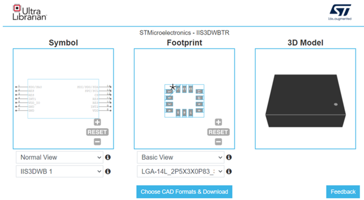
if you go on the st.com page of IIS3DWB device, you can find a session named CAD&Resources, where you can find the CAD symbol, footprint and 3D model.

In case you want to build by your own footprint, I suggest you to refer to the PCB design guidelines for ST MEMS sensors (microphone excluded) that you can find in the Technical note TN0018, p.4.
Let me please know if it is enough for your purposes and, in case, please mark this answer as "best".
-Eleon
- Mark as New
- Bookmark
- Subscribe
- Mute
- Subscribe to RSS Feed
- Permalink
- Email to a Friend
- Report Inappropriate Content
2021-02-12 12:07 AM
Hi @NAnand1 ,
if you go on the st.com page of IIS3DWB device, you can find a session named CAD&Resources, where you can find the CAD symbol, footprint and 3D model.

In case you want to build by your own footprint, I suggest you to refer to the PCB design guidelines for ST MEMS sensors (microphone excluded) that you can find in the Technical note TN0018, p.4.
Let me please know if it is enough for your purposes and, in case, please mark this answer as "best".
-Eleon
- Mark as New
- Bookmark
- Subscribe
- Mute
- Subscribe to RSS Feed
- Permalink
- Email to a Friend
- Report Inappropriate Content
2021-02-12 01:02 AM
BEST!
Many thanks, Eleon
- Machine Learning method and tools for VL53L8CX and VL53L8CH in Imaging (sensors)
- STSW-IMG040 and STSW-IMG-035 - API Footprint RAM and FLASH consumption in Imaging (sensors)
- Cadence Footprint or CIS symbol about VL53L5CX in Imaging (sensors)
- suggested land pattern for Part no:LSM6DSLTR in MEMS (sensors)
- LPS28DFW and VL53L4CD 3D CAD Models in Imaging (sensors)