- STMicroelectronics Community
- Product forums
- Power management
- IHM08M1 - Issues with the Over Current Protection ...
- Subscribe to RSS Feed
- Mark Topic as New
- Mark Topic as Read
- Float this Topic for Current User
- Bookmark
- Subscribe
- Mute
- Printer Friendly Page
IHM08M1 - Issues with the Over Current Protection (OCP)
- Mark as New
- Bookmark
- Subscribe
- Mute
- Subscribe to RSS Feed
- Permalink
- Email to a Friend
- Report Inappropriate Content
2021-02-04 08:31 AM
Hello all,
I am developing a position control for a 48V BLDC motor here. The hardware I'm using is an IHM08M1 motorshield and a NUCLEO-H743ZI2 microcontroller board. Since I use the Ethernet functionality of the Nucleo board (and the RMII has overlaps with other pins), the two boards are not plugged to each other but initially only wired with the necessary pins.
Now I am sitting in front of two blown MOSFETS (phase A) on the motor board. Actually the OCP should pull the BKIN pin from logical 3.3V to GND when the current is greater than 30A. Which would then cause the PWM signal at timer 1 to be turned off
See UM1996 (Getting Started with the IHM08M1). On page 17/29 the following is written: "Over Current Protection (OCP) is implemented by hardware with a detection circuit. The current is compared with an embedded current reference (by the MCU) and the output generates a fault condition at the BKIN pin that goes to ground. This pin, connected to STM32 Nucleo board (BKIN Timer function), detects this condition and immediately disables the driving signals (see the schematic below)."
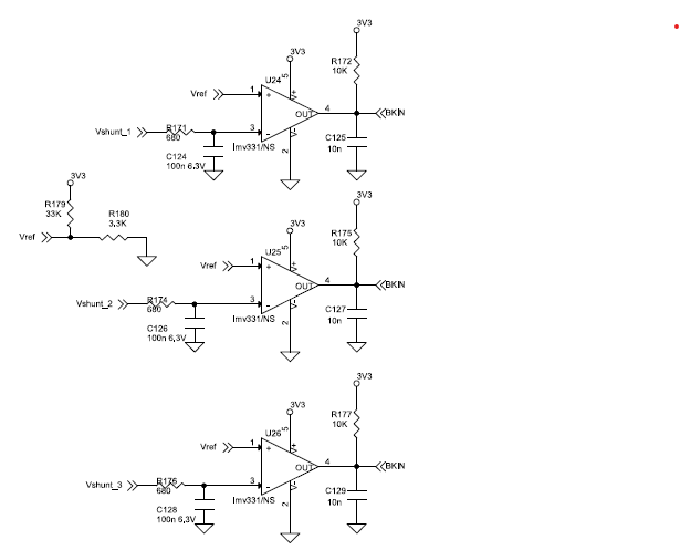
According to Figure 12, the electronic circuit is as follows:

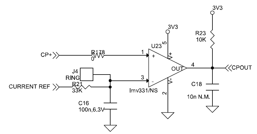
Unfortunately this mechanism does not work. Even at a current of 40A BKIN is still HIGH (3.3V). That's why the transistors of one phase have been destroyed in case of a controller fault now. I made a cross check by applying for the signal CURRENT_REF at pin PB4 (CN10_27) the for 30A corresponding reference voltage (30A*Rshunt*5.18). As soon as this current is exceeded, CPOUT at pin PA12 (CN10_12) switches from GND to 3.3V. So the current is obviously detected correctly via the shunt resistor (which is also confirmed by the readout of the Curr_Fdbk signals at the ADC).
Does anyone have any idea why the BKIN protection mechanism is not triggering properly?
Since I can't plug the boards on top of each other, could possibly the fault be in a non-transmitted signal (the wording with the specified signal by the MCU for the OCP in the UM1996 confuses me)?
The OCP circuit actually only needs the 3.3V supply voltage from MCU and IHM08M1 (pin C7_12) to work properly?
- Labels:
-
Motor Control Hardware
- Mark as New
- Bookmark
- Subscribe
- Mute
- Subscribe to RSS Feed
- Permalink
- Email to a Friend
- Report Inappropriate Content
2021-02-16 05:53 AM
Hello @JSteg.2 and welcome to the ST Community.
You are right the reference voltage Vref for the OCP is set through the R179/R180 voltage divider.
In the X-NUCLEO-IHM08M1 board all the MCU signals and power pins are available on the ST morpho connector.
The BKIN signal is mapped to the connector CN10 on three different pins: C10_13, C10_14 and C10_28.
According to your STM32 Nucleo-64 board you can use the proper connection through the available solder bridges.
You are using a STM32 Nucleo-144 control board, in the NUCLEO-H743ZI2 you must connect the BKIN signal to the PE15 (TIM1_BKIN1 signal) at CN10_30 of Zio connector or to CN12_53 of ST Morpho connector (not soldered by default).
When you check the BKIN triggering, is the 40 A the total load current?
Keep in mind that the total current could split between half-bridges and therefore not trigger the OCP.
Let me know if these info are useful to you.
- Mark as New
- Bookmark
- Subscribe
- Mute
- Subscribe to RSS Feed
- Permalink
- Email to a Friend
- Report Inappropriate Content
2021-02-16 12:16 PM
*So sorry, something went wrong with the pictures in my answer. Maybe you can delete the previous post (I tried, but could not do it).*
Hello Christiana,
Thank you very much for your answer!
You are right the reference voltage Vref for the OCP is set through the R179/R180 voltage divider.
Perfect!
In the X-NUCLEO-IHM08M1 board all the MCU signals and power pins are available on the ST morpho connector. The BKIN signal is mapped to the connector CN10 on three different pins: C10_13, C10_14 and C10_28. According to your STM32 Nucleo-64 board you can use the proper connection through the available solder bridges.
This is exactly how I understood it. According to figure 10 on page 15 in UM1996 the outputs of all three OCP circuits are connected (resistors R73, 74 and 78 are all soldered in the delivery state of the IHM08M1). That means triggering one of these three comparator circuits from my first post (detect an Overcurrent by HW) would also affect all three pins equally (pull all from HIGH to LOW)?

You are using a STM32 Nucleo-144 control board, in the NUCLEO-H743ZI2 you must connect the BKIN signal to the PE15 (TIM1_BKIN1 signal) at CN10_30 of Zio connector or to CN12_53 of ST Morpho connector (not soldered by default).
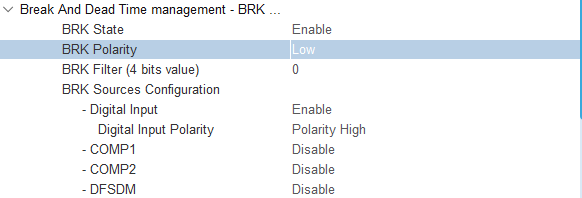
I have connected pin C10_13 (PA6) of the IHM08M1 to pin C12_16 (PB12) of the NUCLEO-H743ZI2 Morpho Connector (soldered the pin rows by myself) configured as TIM1 BKIN1. The BRK polarity is set to LOW.

I think this configuration should actually do it. Nevertheless, even with the test load of 40 A and the voltage measurement of pin C10_13 (PA6) of the IHM08M1 with an oscilloscope, no OCP signal was detected here (edge from HIGH to LOW).
When you check the BKIN triggering, is the 40 A the total load current? Keep in mind that the total current could split between half-bridges and therefore not trigger the OCP.
I'm pretty sure the 40A is the complete load current.
Firstly, because the comparator circuit shown in Figure 9 (page 14) works reliably after set a corresponding CURRENT_REF Signal (e.g. for 30A):

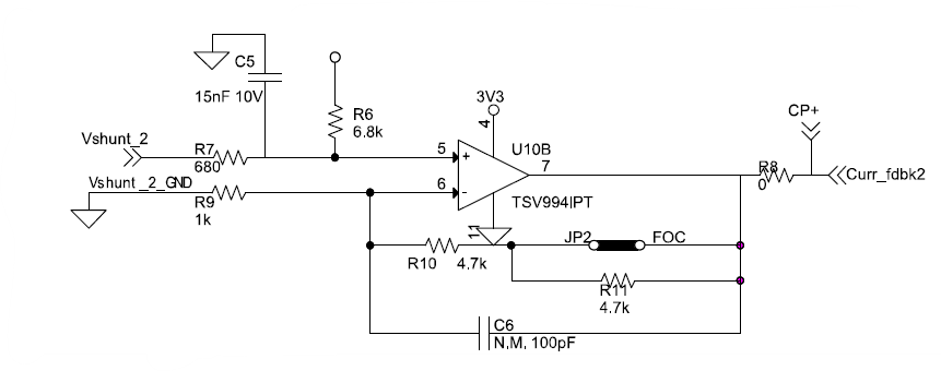
CP+ here is identical to the the voltage point Curr_fdbk2, which in turn is the output of the current measurement circuit with input voltage Vshunt_2 (Figure 9, page 14):

Vshunt_2 is also the rerference signal for the middle OCP circuit with BKIN as output (see the picture in my first post). Vshunt_2 drops across shunt resistor R44 (Figure 13, page 18):


If I have understood all this correctly, the entire load current in this 1Sh configuration thus flows at all times via the point Vshunt_2 or respectively through the shunt resistor R44. Independent of the switching state of the three half bridges. Because between the fictitious ground of the pulse inverter bridge (SENS1-3) and the actual GND there are still the shunt resistors R43-R45. Depending on the connection in J5 and J6, these resistors are either connected to the active motor phase in the 3Sh configuration, and are only energized when the lower transistor of the corresponding half bridge is active. Or, as already mentioned, in the Sh1 configuration the entire current is always conducted via R44 (Phase 2).
Please correct me if I am wrong somewhere with my assumptions.
Do I need to remove any resistors perhaps? I am confused by the fact that all three outputs of the OCP circuits (picture last post) end at the same voltage point BKIN. Which according to Figure 10 is connected to all three pins. In a 1Sh configuration, wouldn't the two unused OCP circuits (phase 1 and 3) always pull the BKIN signal HIGH (regardless of whether the OCP circuit of phase 2 has detected an overcurrent and set its output to LOW). Or is a LOW output sufficient to automatically pull BKIN to GND (regardless of what the other two circuits have as output)?
Maybe my board simply has a manufacturing defect in the OPC circuit. I have already ordered more boards. Unfortunately, there seem to be strong delivery problems on the part of STM at the moment. Is it foreseeable when the boards can be shipped to the dealers again (I know, that's a bit far away from the original topic now)?
Thanks in advance for your effort!
- Mark as New
- Bookmark
- Subscribe
- Mute
- Subscribe to RSS Feed
- Permalink
- Email to a Friend
- Report Inappropriate Content
2021-02-25 05:41 AM
Hello @JSteg.2,
concerning to the BKIN signal, usually one of the three C10 pins of the X-NUCLEO-IHM08M1 is kept solder according to your STM32 NUCLEO (the others two removed e.g. R73 and R74).
In your case the important thing is one of them is correctly mapped in your TIM1 BKIN port (PB12). The polarity active low is right.
The "OCP circuits" that generates BKIN signal are made with comparators with open-drain outputs suitable for wired-OR application, so it only one of the three comparator outputs goes low to pull-down the BKIN signal.
My previous question about the total load current assumed a 3Sh configuration.
If you are working in single shunt topology (J5 and J6 closed on Vshunt_2) your assumptions are all correct. It is not necessary remove any shunt resistor.
Besides, I can't help you with the boards delivery.
For the moment I can only advise to review if all the other signals you need to drive the board correctly have been connected properly (refer to section 2.2.1 of the UM1996 and in particular to Table 3 and 4).
Let me know when you are able to make new tests.
- MotionMC running algo but no output bias data calculated (all to default) in STM32 MCUs Embedded software
- OCP in custom board in STM32 MCUs Motor control
- b-g431b-esc1 Overcurrent at the start in STM32 MCUs Motor control
- Why I_Q_MEAS is zero when motor is locked and I_Q_REF goes up to the maximum value? in STM32 MCUs Motor control
- STM32F429 GPIO 5V tolerant IO behavior in STM32 MCUs products