- STMicroelectronics Community
- STM32 MCUs
- STM32 MCUs Wireless
- Matching Network Design Confirmation & Questions
- Subscribe to RSS Feed
- Mark Topic as New
- Mark Topic as Read
- Float this Topic for Current User
- Bookmark
- Subscribe
- Mute
- Printer Friendly Page
Matching Network Design Confirmation & Questions
- Mark as New
- Bookmark
- Subscribe
- Mute
- Subscribe to RSS Feed
- Permalink
- Email to a Friend
- Report Inappropriate Content
2020-12-09 10:01 PM
After going through AN5457 I want to confirm whether I have correctly followed the design guidelines presented.
I am aiming at 920MHz and have used the 923MHz 22 dBm value for Z0 (10.58-j10.71).
This is my first time dealing with RF but I understand that the aim is to reach the center of the smith chart and hence 50/0 Re/Im. On page 26 it gets a bit confusing as the notch filter chart clearly moves away from the 50 Ohm center point. This is the last chart in the document which shows the full network so I'm not sure if the remaining components are supposed to return to the center or not.
I have assumed that the end result should return to the center and therefore be as close to 50/0 as possible upon entering the RF switch. Is this the correct outcome or are the filtering stages not expected to return to the 50 Ohm value?
My smith chart and matching circuit are attached. All values on the components for Q are extracted from the murata SimSurfing tool.
I also have a few other questions:
- Why does the power level affect the load-pull impedance value when the frequency is the same?
- If designing for both low and high power from a single RFO pin (e.g. 17 or 22 dBm from RFO_HP, 10 or 15 dBm from RFO_LP) which PA impedance should be used for the matching network design? (i.e. highest power, lowest power, in-between etc.)
- The matching network of the high band (868/915) Nucleo doesn't seem to follow the AN5457 guidelines. Was AN5457 finished after the Nucleo design was finalized or is there another reason?
- Labels:
-
STM32WL Series
- Mark as New
- Bookmark
- Subscribe
- Mute
- Subscribe to RSS Feed
- Permalink
- Email to a Friend
- Report Inappropriate Content
2021-01-06 02:24 AM
Hi @David Orr ,
My best wishes for 2021.
I'll try to answer each question.
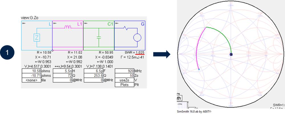
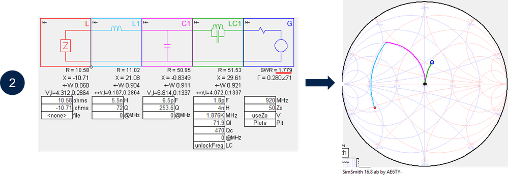
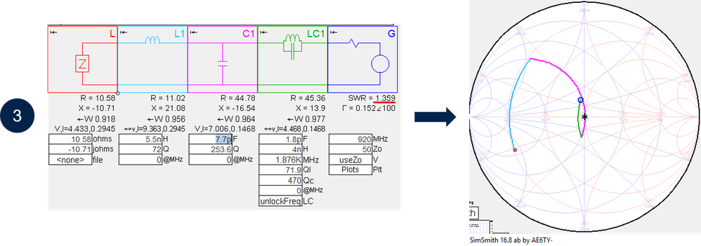
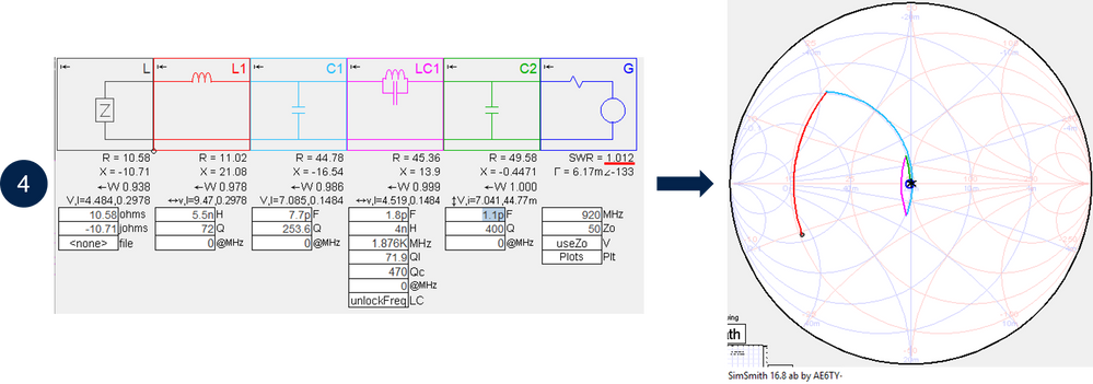
1) Generally the input impedance of the antenna is 50 ohms. Thus, after filtering stages, the output impedance of the network (towards antenna) should be equal to 50 ohms to ensure the maximum energy transfer to be radiated. I've attached some images to show you step by step this procedure from the impedance value chosen by you. I applied steps 1 and 3 on page 27 to get the attached images. Note that in these images the antenna is represented by the 920 MHz source (on the right) with an impedance value of 50 ohms. The VSWR is the one seen by the antenna. Remember that in this exercise, the goal is to minimize the VSWR seen by the antenna as much as possible.
2) An RF Power Amplifier (RF PA) is a non-linear device and cannot be characterized only by S-parameters. In order to determine the best trade-off in overall performance of the RF PA, we present various load impedance values to the PA in a precisely and controlled characterization analysis called load-pull (or source-pull for the LNA). This analysis is performed at various bias and frequency conditions. When we configure an RF output power value, the device internally changes the bias conditions of the RF PA, consequently changing the output voltage and current values and, therefore, its equivalent output impedance. So, to summarize, when configuring the RF output power value you change the device operating conditions.
3) FYI, in the context of this product we usually use the terms "high power" for values > +15 dBm and "low power" for values < +15 dBm. Changing the RF output power value from +22 dBm to +17 dBm makes sense if you also change the PA's optimal settings, otherwise the power consumption will not change significantly as if you had programmed the corresponding optimal setting. But, for each optimal settings, you need a dedicated matching network. Why do you need this "adaptive RF power"? If you are trying to control the amount of energy generated/spent during the RF transmission, for this purpose, in the LoRaWAN protocol, you change the data rate of the communication by modifying the Bandwidth, Spreading factor and Coding Rate. But if you want to design an application with a kind of "adaptive RF power" (same matching network and optimal setting, but changing only the configured power values), I would say to use the impedance value corresponding to the highest power value. For a different power value you can obtain the expected value (or some value close to that) even using a matching network of another RF power/impedance, but with extra current consumption compared to an optimal setting with its dedicated matching network. The extra consumption is mainly due to circuit losses. It's important to ensure the VSWR (at RFO pin) do not exceed 10:1 when using a different matching network for a different power value. To avoid internal thermal issues (due to loss) when doing an adaptive RF power, I recommend using a TCXO as HSE clock source instead of XO. Thermal dissipation inside the device may cause frequency drift problems.
4) There are some reasons. First, I wrote AN5457 after the Nucleo Board. Another reason is the PCB. It can add considerable impact to component values. I strongly recommend to perform the step-by-step described in AN5457 for your PCB after replicating the matching network values for the entire production. By doing that you will see for each step how your PCB changes the impedances seen by the device and by the antenna and you will be able to determine the exact values to be implemented starting from the calculated values described in the AN5457. Note that this procedure requires the DUT and a spectrum analyzer to measure the power of fundamental frequency (H1) and harmonics (H2, H3, H4...). There is also another reason why the RF BoM values change. It's because we use advanced techniques combined with measurements made with expensive RF equipment in our Labs in order to determine the minimal BoM. If you don't have access to RF tuners, VNAs, spectrum analyzers and VSGs, or a solid background in this area, you really need to follow a strict theoretical procedure combined with a fine-tuned implementation on your PCB in order to to determine the corresponding network values otherwise it quickly becomes a nightmare. Note that if you copy and paste the RF layout part of the Nucleo board with the same PCB substrate, you can use the component values of the Nucleo Board as they match that layout/substrate well. If you do not exactly copy the RF layout and substrate of a given boad such as Nucleo Board or Reference Design Board provided by ST, you must apply the procedure described in AN5457 to determine the corresponding network values. FYI ST provides also some Reference Design Boards + RF BoM with an RF optimized layout.
Let me know if this answers your questions.
Kind regards,
Hamilton

(Combining the values of C2 and C3 and adding DC block capacitor)

STM32WL
- Mark as New
- Bookmark
- Subscribe
- Mute
- Subscribe to RSS Feed
- Permalink
- Email to a Friend
- Report Inappropriate Content
2021-01-06 10:52 PM
Thanks for the detailed reply @Hamilton DC, and a happy new year to you too. Your explanation really helps with many of the doubts that have occurred as a result of my own inexperience.
My device is for an honors thesis project and is my first ever electronic design, so everything has been self-taught over the past 3-4 months. It's also my first experience with STM32 devices so there has also been a knowledge gap compared to someone that has worked with other devices in the STM32 family.
The device is based on the STM32WL and powered by energy harvesting (using ADP5091 PMIC) so having adjustable power settings is very helpful to provide a way of reducing energy usage when distance is lower. Simply having separate low and high power TX pathways definitely goes a long way toward this goal though.
I did some further study and found the same conclusion that you stated about the non-linearity of the PA. It's unfortunate that it behaves this way since things could be much simpler if it were a linear relationship, but that's just the way it is.
After some investigation I also became convinced that my suspicion about the 50 Ohm value was correct, which you have confirmed. i found it easiest to tune the network by trying to maximize return loss as I feel it is easier to see in SimSmith.
There is a possibility that I will have access to a VNA at some point but currently I am limited to theoretical methods, though I am getting more confident in the reliability of my work so far (especially now with your information).
I have gone through as much reference material as I could find and have been trying to apply as much "best practice" as I can find to ensure good results. My final matching network is based mainly on the NUCLEO layout because of the 3-way RF switch and it looks like this:
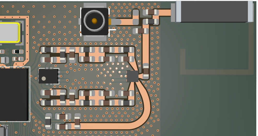
- I have kept mask off the GCPW lines to help control the dielectric coefficient. My main concerns are the corners (through components) leading to the antenna/u.FL as I'm not sure what impact that has on the signal, but it's something I've seen on professionally designed boards and helps save space.
- I am also using a TCXO (TG2520SMN 32.0000M-ECGNNM3).
- The PA goes through a TS3A52 DP/DT switch (on the left) instead of 2 discrete switches like in the MB1389D design.
For the actual matching network, I have used the thickness/dielectric values from the MB1389D gerber stackup to add the PCB effects to the SimSmith by adding a transmission line between each component and taking the length from the PCB layout:

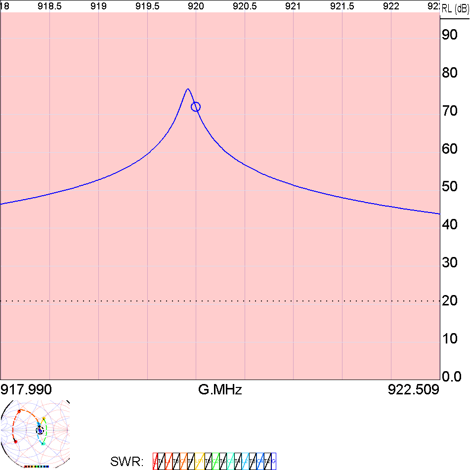
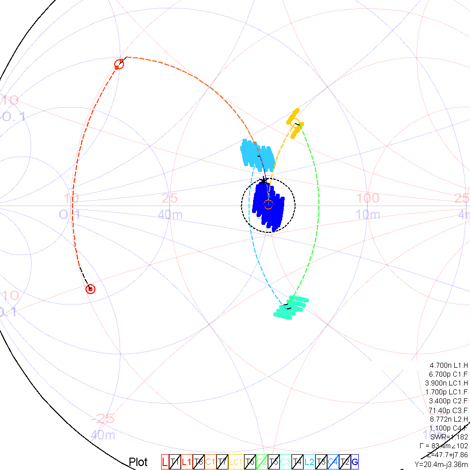
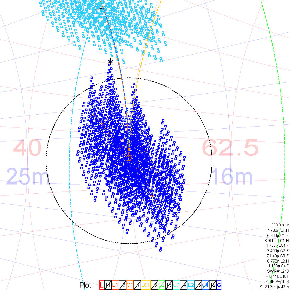
I was finally able to get my hands on a pair of NUCLEO-WL55JC1 boards two days ago and have been able to make some progress learning the syntax and programming structure, though it's harder than I was expecting. My aim is to dig into any aspect of the system that I have any doubts about to make sure my design is correct.
One thing I have had a lot of trouble with is the dual core stuff. I went though AN5564 but can't seem to launch the M0+ CPU as it throws an "Error 32" when trying to make the ST-LINK connection. My interpretation of the launch steps is to "debug" on the M4 subproject --> hit resume and wait to reach infinite while loop (to set the C2BOOT bit) --> "run"/"debug" on the M0+ subproject.
I'd appreciate any insight into this issue, and thanks again for your help.
- STM32WL55/STM32WLE5 SubGHz in STM32 MCUs Wireless
- An issue with the custom hardware in p2p and LoRaWAN mode in STM32 MCUs Wireless
- How to flash STM32H725 using FDCAN Bootloader? in STM32 MCUs Embedded software
- STLINK-V3SET: Question About Adapter Board to Program via SWD in STM32 MCUs Boards and hardware tools
- I have a question about the STM32G031. I want to confirm that the 28 pin package can be programmed using pins 18 and 19 with uart? in STM32 MCUs Embedded software
