- STMicroelectronics Community
- Product forums
- Power management
- L6699 Enhanced high voltage resonant controller. A...
- Subscribe to RSS Feed
- Mark Topic as New
- Mark Topic as Read
- Float this Topic for Current User
- Bookmark
- Subscribe
- Mute
- Printer Friendly Page
L6699 Enhanced high voltage resonant controller.
App Note AN4027 - Question on L6699 timing circuit.
- Mark as New
- Bookmark
- Subscribe
- Mute
- Subscribe to RSS Feed
- Permalink
- Email to a Friend
- Report Inappropriate Content
2020-11-27 07:03 PM
This App Note is identified by the following meta-data:
Identifiers: AN4027, Doc ID 022604 Rev 1
Title: "12 V - 150 W resonant converter with synchronous rectification using the L6563H, L6699 and SRK2000"
Author: Claudio Spini.
Date: July 2012
Hello Sir/Madam,
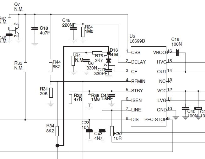
Question 1: The schematic on page 12/38 shows a connection between D16K & R34. (Note: D16 anode is connected to L6699 pin 3, CF). That connection is marked "connection made by re-work". I seek an explanation as to why this connection was done.
Question 2: Several components on the schematic are marked "N.M.", eg: D16, C43. What does "N.M." mean?
Many thanks!
Edit 02-Dec-2020: Added image below, the relevant portion of the schematic.
Solved! Go to Solution.
Accepted Solutions
- Mark as New
- Bookmark
- Subscribe
- Mute
- Subscribe to RSS Feed
- Permalink
- Email to a Friend
- Report Inappropriate Content
2021-01-11 12:44 AM
Hello @FBaro.1,
Q1:
L6599 and L6699 have the same oscillator section.
The mentioned components are for L6599A only, not intended to be used for L6699.
Concerning the oscillator of new device you can refer to the L6699 datasheet at page 17: section 6.3 Safe-start procedure.
Q2:
You can always find the explanation in the L6699 datasheet (6.3 section).
The added components of L6599A provide for an asymmetry of the oscillator triangle, providing a different duty among LVG and HVG signals to prevent initial current peaks at turn on.
The soft start pin can increase the frequency during soft start but with symmetrical duty only.
The L6699 overcomes the issue.
Let me know if I solved your doubts.
- Mark as New
- Bookmark
- Subscribe
- Mute
- Subscribe to RSS Feed
- Permalink
- Email to a Friend
- Report Inappropriate Content
2020-12-01 07:46 AM
Hello @FBaro.1 and welcome to the ST Community.
Concerning your question:
- The "re-work" connection add an RC network in parallel to the optocoupler transistor in order to guarantee the loop regulation stability under all conditions.
- N.M. is the acronym of Not Mounted
If I answered your questions please "Select as Best" button.
- Mark as New
- Bookmark
- Subscribe
- Mute
- Subscribe to RSS Feed
- Permalink
- Email to a Friend
- Report Inappropriate Content
2020-12-01 10:25 AM
Hello Cristiana,
Thanks for explaining that "N.M." means "Not Mounted" - this is equivalent to the term that we use, which is: "DNL" = "Do Not Load".
So, that means that D16 does not exist on the actual board that was tested in the app note, and therefore it is now very clear that R16 and C6 simply provide stability for the feedback loop. Great, thanks for that.
However, I am still intrigued by D16, and I would be very interested to know the intent of the original designer by the connection of D16 anode to L6699 pin 3 (CF), since pin 3 is the timing waveform, which will be a triangle wave, oscillating between 0.9V & 3.9V in time with the switching frequency. I am very surprised that such a connection was drawn on the schematic in the first instance, since any disturbance to the current to the capacitor on this pin will change the control characteristics of the L6699. Since C6 (330nF) is much larger than C17 (330pF), then perhaps this was intended either:
(a) to force the switching frequency to be very low at power up
(b) as a F to V converter, ie: dc voltage on C6 was a function of switching frequency, as a means to observe Fs?
Or perhaps neither of these are correct - maybe you may have a better idea what the original intention was? I have not seen any schematic of the L6599 or L6699 where the timing cap (pin 3) had any other component connected other than the timing capacitor.
Cheers,
-F.Barone.
2020-12-12 Edit: deleted image since this was already in the original question.
- Mark as New
- Bookmark
- Subscribe
- Mute
- Subscribe to RSS Feed
- Permalink
- Email to a Friend
- Report Inappropriate Content
2020-12-22 06:45 AM
Hello @FBaro.1,
I didn’t forget your questions 😉
I am trying to get in contact internally with the expert of this product. I hope to be able to answer your doubts as soon as possible.
- Mark as New
- Bookmark
- Subscribe
- Mute
- Subscribe to RSS Feed
- Permalink
- Email to a Friend
- Report Inappropriate Content
2021-01-03 06:44 PM
Ciao Cristiana,
buon Natale & felice anno nuovo.
Just wondering have you been able to make contact with your expert?
Grazie mille!
- Mark as New
- Bookmark
- Subscribe
- Mute
- Subscribe to RSS Feed
- Permalink
- Email to a Friend
- Report Inappropriate Content
2021-01-07 06:24 AM
Hello @FBaro.1 Happy New Year to you too.
The PCB mounting option (D16, R16, R4, C6) is not used for L6699 IC.
The same PCB is shared with a older device (L6599A) that could use this mounting option (useful for oscillator start-up phase).
If we can consider closed this topic please "Select as Best" button in the proper reply to the original question.
- Mark as New
- Bookmark
- Subscribe
- Mute
- Subscribe to RSS Feed
- Permalink
- Email to a Friend
- Report Inappropriate Content
2021-01-07 03:40 PM

thanks for your reply.
Just to explain the reason for my questions: we are currently using the older device (L6599), and are interested to learn what benefits the newer device (L6699) offers us in our particular application. So I wish to understand this issue better before moving on to investigate the other features of the newer device that are different to the older device.
So, the main purpose of this question is really to understand any differences between these two devices in regards to pins 1, 3 & 4.
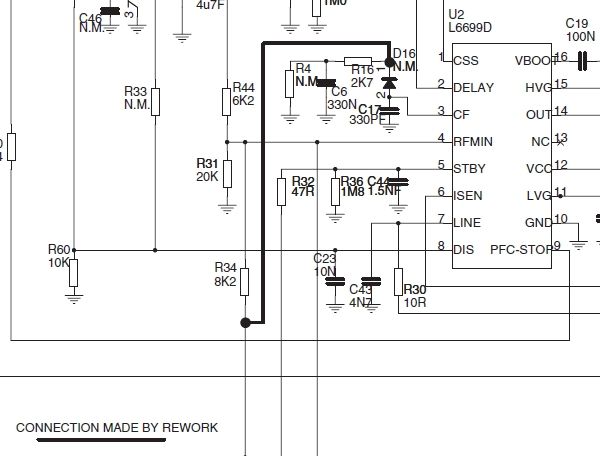
Please note: I have attached here a larger image of the same schematic; this new image includes C18, as this component now becomes part of the discussion.
Question 1:
My understanding of the two devices (L6599 & L6699) is that they have the same oscillator section (associated with pins 1, 3, & 4).
Is my understanding correct, or am I mistaken?
If my understanding is correct, then why would these components (D16, R16, R4, C6) only be useful for the older device, and not useful for the newer device?
If my understanding is not correct, then please point me to a link where I can learn how the oscillator section of the new device is different to the older device.
Question 2:
From your answer, it would seem that these components (D16, R16, R4, C6) were intended to provide some kind of control over the start-up phase of the oscillator. We also know that the soft-start function (pin 1, C18) on the older L6599 is not just involved in start-up, but is also involved in overload protection (refer DocID15534 Rev 8, June 2017, section 6.4, pages 19 to 23). So, it would seem, and this is just my guess, that the original designer intended these components (D16, R16, R4, C6) to allow the start-up behaviour to be different to the over-load behaviour.
However, when these components are mounted, they can only remove current from pin 3 in one direction - and this is my main concern, as I will try to explain below:
Under normal operation, the current flowing out of pin 3 changes direction: it is positive (flows out of pin 3) to cause C17 voltage to rise, and it is negative (flows into pin 3) to cause C17 voltage to fall. These currents must have the same amplitude but opposite polarity, otherwise the duty-cycle of the oscillator will not be 50%, and this will cause the output drive to the main MOSFETs to become unbalanced (not 50% duty cycle).
For normal operation, the voltage on C17 is a triangle wave that has equal rise and fall times. However, any current flowing in D16 will cause the charging and discharging currents in C17 to become unbalanced, which causes the voltage on C17 to become unbalanced: the rise time will be longer, and fall time will be shorter.
I am concerned that when the duty-cycle of the timing waveform (C17 voltage) is no longer balanced at 50%, then the drive signals to the MOSFETs also become unbalanced. This is not a mode of operation that I have seen described anywhere.
So, after that rather long introduction (sorry), my question then is:
Q2A: Regarding my understanding of the behaviour of C17 when components (D16, R16, R4, C6) are loaded, is my understanding correct?
Q2B: If my understanding is correct (ie: that components (D16, R16, R4, C6) do actually affect the duty cycle of the gate drive to the main MOSFETs), then is this a valid mode of operation, and is this mode described anywhere?
Regards,
-F.Barone.
- Mark as New
- Bookmark
- Subscribe
- Mute
- Subscribe to RSS Feed
- Permalink
- Email to a Friend
- Report Inappropriate Content
2021-01-11 12:44 AM
Hello @FBaro.1,
Q1:
L6599 and L6699 have the same oscillator section.
The mentioned components are for L6599A only, not intended to be used for L6699.
Concerning the oscillator of new device you can refer to the L6699 datasheet at page 17: section 6.3 Safe-start procedure.
Q2:
You can always find the explanation in the L6699 datasheet (6.3 section).
The added components of L6599A provide for an asymmetry of the oscillator triangle, providing a different duty among LVG and HVG signals to prevent initial current peaks at turn on.
The soft start pin can increase the frequency during soft start but with symmetrical duty only.
The L6699 overcomes the issue.
Let me know if I solved your doubts.
- Mark as New
- Bookmark
- Subscribe
- Mute
- Subscribe to RSS Feed
- Permalink
- Email to a Friend
- Report Inappropriate Content
2021-02-10 06:03 AM
Hello @FBaro.1,
we can consider close this topic?
If so, please "Select as Best" button in the proper answer to your original question.
- Mark as New
- Bookmark
- Subscribe
- Mute
- Subscribe to RSS Feed
- Permalink
- Email to a Friend
- Report Inappropriate Content
2021-02-10 12:33 PM
Thank you Cristiana, yes, my questions were answered by the reference you provided (datasheet for L6699 at page 17: section 6.3 Safe-start procedure.)
Thanks again!
- Can we use L6559D LLC controller with out a active PFC controller in a AC to DC SMPS applications? in Power management
- General Purpose Timers: what are the options for One-Pulse slave mode trigger? in STM32 MCUs products
- Need Help for BootLoader in STM32F407xx in STM32 MCUs Embedded software
- [STM32L496] Jumping from bootloader to user Application with RDP enabled doesn't work without going through a power cycle. in STM32 MCUs Security
