- STMicroelectronics Community
- Product forums
- Other: hardware
- Applying voltage to the output pin of STMPS2171STR
- Subscribe to RSS Feed
- Mark Topic as New
- Mark Topic as Read
- Float this Topic for Current User
- Bookmark
- Subscribe
- Mute
- Printer Friendly Page
Applying voltage to the output pin of STMPS2171STR
- Mark as New
- Bookmark
- Subscribe
- Mute
- Subscribe to RSS Feed
- Permalink
- Email to a Friend
- Report Inappropriate Content
2020-10-16 06:23 AM
Hi,
Currently, I have two boards that contain a 5 volt power supply. Due to flexibility for future projects, both of are powering the same pin on a connector. The STMPS2171STR was added to one of the boards to cut the voltage going to the connector.
However, during bring up I checked the impedance of the output pin of the STMPS2171 to ground and it was high, this matched the datasheet. Once the board was powered on (enable off), I noticed that I had current flowing into the STMPS2171STR , when measured and it was roughly 10mA. I decided to recheck the resistance to ground and surprisingly enough I had 1kOhm to ground. I turned off my power supply and the impedance stayed roughly the same. This behavior goes against what section 3.4 of the datasheet.
I have a few questions about this component.
I am using this IC correctly?
I tested a total of 3 different boards, and all of them display a similar behavior. However, the boards were build by hand, How resistant to heat are those ICs?
The datasheet states that this device is 8kV ESD rated, is this correct?
some more information:
The IC used on the other board supplying the 5V is the LMR34206FSC5RNXRQ1
Thank you,
Matheus Oliveira
Solved! Go to Solution.
- Labels:
-
Switches and Multiplexers
Accepted Solutions
- Mark as New
- Bookmark
- Subscribe
- Mute
- Subscribe to RSS Feed
- Permalink
- Email to a Friend
- Report Inappropriate Content
2020-10-27 12:43 AM
Sometimes it is not easy to follow the thoughts when the parameters of the given environment are not fully known or visible. In your case, it is an overview of which voltage (+5VDC_SWITCHED, 24VDC) is present and when.
But anyway - the STMPS21x1 are primarily designed as a power switch and blocks reverse current under certain conditions - but not all. What I can see so far you really need a full separation of the voltages (+5VDC_SWITCHED, 5VDC), which can be achieved using:
- two STMPS21x1, as mentioned before
- diodes (preferably Schottky) from each of the voltages towards the load, which includes losses due to voltage drop
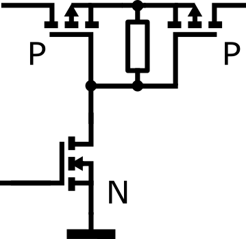
- 2 p-channel logic level MOSFETs connected anti serial (see example attached)
Does it answer your question now?
/Peter
- Mark as New
- Bookmark
- Subscribe
- Mute
- Subscribe to RSS Feed
- Permalink
- Email to a Friend
- Report Inappropriate Content
2020-10-19 02:55 AM
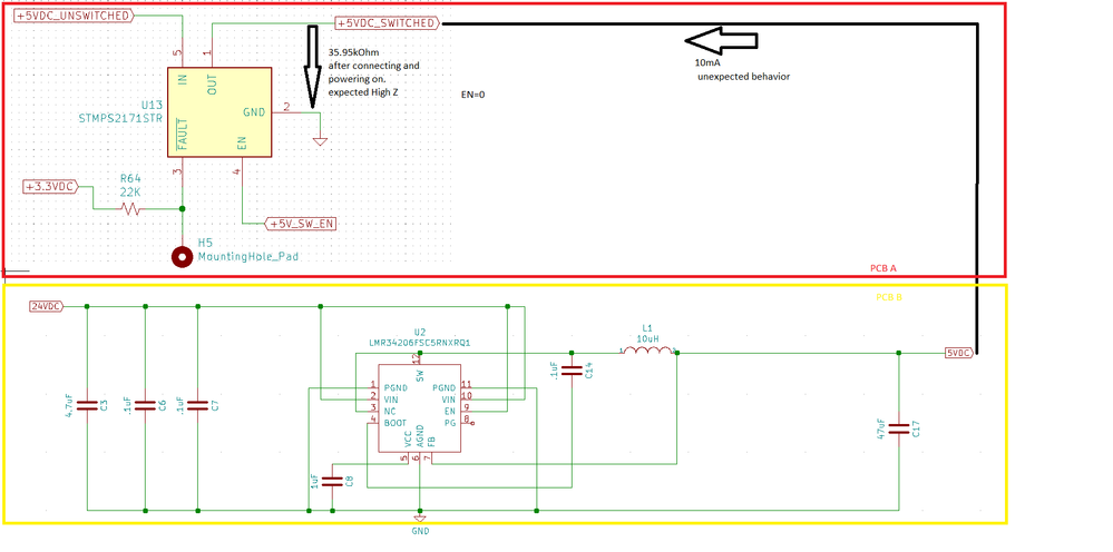
Please provide a schematic of your setup to make sure we understand it correctly.
Regards
/Peter
- Mark as New
- Bookmark
- Subscribe
- Mute
- Subscribe to RSS Feed
- Permalink
- Email to a Friend
- Report Inappropriate Content
2020-10-19 06:21 AM
- Mark as New
- Bookmark
- Subscribe
- Mute
- Subscribe to RSS Feed
- Permalink
- Email to a Friend
- Report Inappropriate Content
2020-10-19 07:51 AM
It looks like you want to connect either +5VDC_UNSWITCHED or +5VDC_SWITCHED to 5VDC, right?
To achieve this, it is probably better to use an STMPS2171 and, in addition, an STMPS2161:
- both OUT pins connected to 5VDC
- both EN pins connected together
- maybe both /FAULT pins connected together (Wired OR)
- the respective IN pins connected to either +5VDC_UNSWITCHED and +5VDC_SWITCHED
The STMPS2161 uses an inverted EN signal, so if you set EN to either Low or High, one of the input voltages will be selected.
Does it answer your question?
/Peter
- Mark as New
- Bookmark
- Subscribe
- Mute
- Subscribe to RSS Feed
- Permalink
- Email to a Friend
- Report Inappropriate Content
2020-10-19 08:27 AM
They are in separate PCBs. I tried using MS paint to separate on the picture, but I think I failed that and I apologize for that.
My goal is to be able to connect the PCB A (inside the red rectangle) to different PCBs. On this scenario both PCBs had a 5V power supply. I wanted to use the 2171 to separate the 5V unswitched from the 5VDC. At the moment the PCB inside the yellow box cannot be modified.
Do you recommend adding a diode on the PCB A (red box) to block the reverse current? I was under the impression from section 3.4 that the output pin would be able to handle this application. PCB A is pretty tight already, and adding more complexities would be challenging.
If the part cannot handle the voltage on the output pin, can I just use a diode on that pin and compensate for the diode drop?
And thank you for the quick response!
- Mark as New
- Bookmark
- Subscribe
- Mute
- Subscribe to RSS Feed
- Permalink
- Email to a Friend
- Report Inappropriate Content
2020-10-26 06:22 AM
I need to send the board out and this IC is holding release. It would be good to know why my PCB is not behaving the way that the datasheet specifies. I have until the end tomorrow to find a solution. I am inclined to go with a diode solution for now, but I would prefer using this part, or a similar power switcher for my application.
Thank you,
Mat. O.
- Mark as New
- Bookmark
- Subscribe
- Mute
- Subscribe to RSS Feed
- Permalink
- Email to a Friend
- Report Inappropriate Content
2020-10-27 12:43 AM
Sometimes it is not easy to follow the thoughts when the parameters of the given environment are not fully known or visible. In your case, it is an overview of which voltage (+5VDC_SWITCHED, 24VDC) is present and when.
But anyway - the STMPS21x1 are primarily designed as a power switch and blocks reverse current under certain conditions - but not all. What I can see so far you really need a full separation of the voltages (+5VDC_SWITCHED, 5VDC), which can be achieved using:
- two STMPS21x1, as mentioned before
- diodes (preferably Schottky) from each of the voltages towards the load, which includes losses due to voltage drop
- 2 p-channel logic level MOSFETs connected anti serial (see example attached)
Does it answer your question now?
/Peter
- Mark as New
- Bookmark
- Subscribe
- Mute
- Subscribe to RSS Feed
- Permalink
- Email to a Friend
- Report Inappropriate Content
2020-10-27 05:46 AM
Yes it does answer my question.
Thank you for your time!
Mat. O.
- Error in initializing ST-LINK device. Reason: No device found on target.(Stm32H755) in STM32CubeIDE (MCUs)
- Broken STM32 in STM32 MCUs products
- SBSFU - can not connect to STM32WB5M - Error: ST-LINK error (DEV_TARGET_CMD_ERR) in STM32CubeProgrammer (MCUs)
- if you apply a supply voltage lower than 3.3V, the ADC will not work. in STM8 MCUs
- STM32G483 ADC Noise when connected to OPAMP PGA Gain -3 in STM32 MCUs products

