- STMicroelectronics Community
- STM32 MCUs
- STM32 MCUs products
- VSSA VDDA and analog / digital ground separation. ...
- Subscribe to RSS Feed
- Mark Topic as New
- Mark Topic as Read
- Float this Topic for Current User
- Bookmark
- Subscribe
- Mute
- Printer Friendly Page
VSSA VDDA and analog / digital ground separation. What's best?
- Mark as New
- Bookmark
- Subscribe
- Mute
- Subscribe to RSS Feed
- Permalink
- Email to a Friend
- Report Inappropriate Content
2020-06-23 02:49 AM
Hello,
I have a mixed signal application in development, a home energy monitor, and following on from the recent PCB version's test results on the effects of noise, and after reading this article, I've decided to separate my digital and analog ground, which makes A LOT of sense.
I have the 100-pin package, STM32F303VE, it has VSSA and VDDA pins. Shall I connect VSSA to analog ground, while connecting VSS (digital) to the digital ground?
I ask because the Analog Dialogue article states that the digital ground of an MCU must be connected to analog ground, for the sampling architecture to have the same reference as the analog elements of the circuit.
However I have reason to believe the sampling architecture of the stm32f3 is connected to VSSA, and therefore can be separated.
I could route all VSS pins to 2-way solder jumpers and could report back with a noise test results on connecting all VSS to either DGND or AGND. If someone already has experience here, I would appreciate the time.
Cheers,
Dan
- Labels:
-
ADC
-
STM32F3 Series
- Mark as New
- Bookmark
- Subscribe
- Mute
- Subscribe to RSS Feed
- Permalink
- Email to a Friend
- Report Inappropriate Content
2020-06-23 04:48 AM
I always tie VSSA directly to VSS at the package and get good performance out of the ADC. If getting the absolute best analog performance is important to you, then you might want to spend time looking at it, but for me at least there's enough to do that spending a lot of effort getting another bit of resolution from the ADC isn't a priority.
I think the more important factor is the quality of your voltage reference and how well isolated VDDA is from noise on VDD.
- Mark as New
- Bookmark
- Subscribe
- Mute
- Subscribe to RSS Feed
- Permalink
- Email to a Friend
- Report Inappropriate Content
2020-06-23 05:21 AM
Okay, so the voltage reference is coming from a dedicated REF19x IC, it can handle a useful amount of capacitance on it's output and the input to VREF therefore looks solid. It appears the REF19x can deliver the current to supply VDDA also – could be a good idea then.
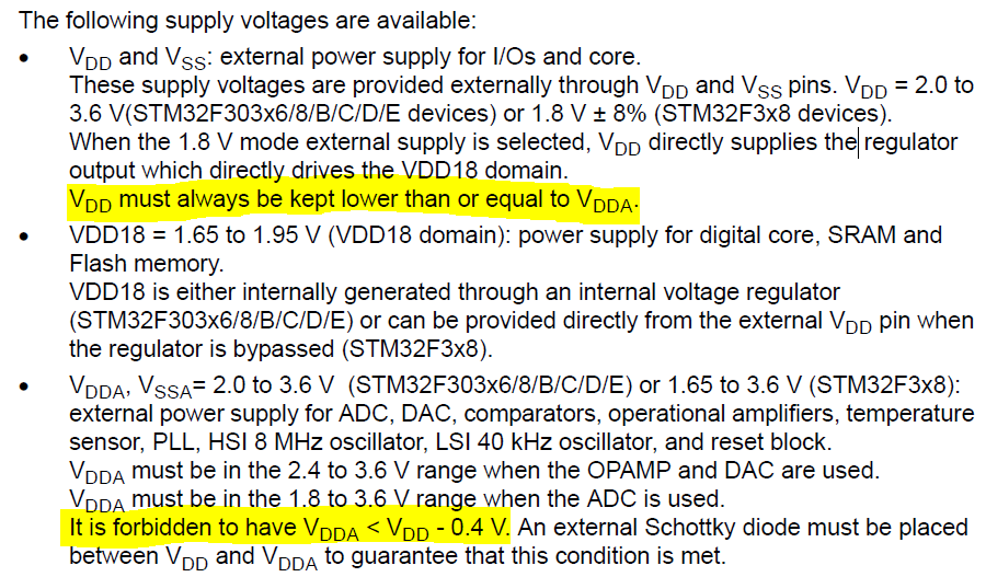
I wonder what would happen if VDDA is slightly higher than VDD, could happen with the tolerance of the regulators, the main one is an MCP1501.
- Mark as New
- Bookmark
- Subscribe
- Mute
- Subscribe to RSS Feed
- Permalink
- Email to a Friend
- Report Inappropriate Content
2020-06-23 05:27 AM
The appnote AN2834 is a good source of information regarding ADC and influencing factors:
https://www.st.com/resource/en/application_note/cd00211314.pdf
Good luck,
/Peter
- Mark as New
- Bookmark
- Subscribe
- Mute
- Subscribe to RSS Feed
- Permalink
- Email to a Friend
- Report Inappropriate Content
2020-06-23 05:30 AM
The reference manual lists some rules for this scheme. Probably other info in there as well.
- Mark as New
- Bookmark
- Subscribe
- Mute
- Subscribe to RSS Feed
- Permalink
- Email to a Friend
- Report Inappropriate Content
2020-06-23 05:38 AM
A useful manual that, I'll have to re-read with an eye to the subject at hand.
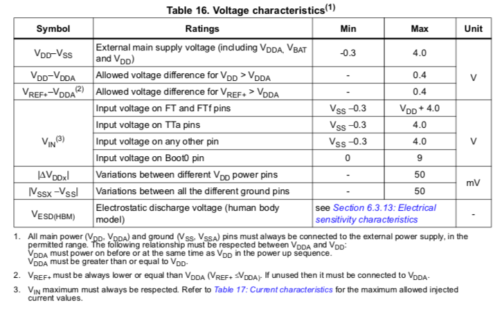
Seems Vdd can go higher than Vdda in terms of maximum ratings. It's the impact on accuracy I'd have to find out.
f303xE datasheet
- Mark as New
- Bookmark
- Subscribe
- Mute
- Subscribe to RSS Feed
- Permalink
- Email to a Friend
- Report Inappropriate Content
2020-06-23 06:13 AM
the ap. note says again and again it's the ratio of VREF+ to the analog input pin that defines the value acquired.
I'll have to get a solder jumper off vdda to test if it prefers the main regulator or the ref19x.
I'll set them both to 3.3V, regardless of the tolerances making an unfavourable condition, seems the chip can handle it.
- Mark as New
- Bookmark
- Subscribe
- Mute
- Subscribe to RSS Feed
- Permalink
- Email to a Friend
- Report Inappropriate Content
2020-06-23 06:49 AM
Any idea what the effect might be if Vdd is slightly higher than Vdda? got a 0.4% difference at 3.3V = 13.2mV difference possible with my comps, MCP1501 is the main reg. I doubt it's important but I'll have to check now :\
- Mark as New
- Bookmark
- Subscribe
- Mute
- Subscribe to RSS Feed
- Permalink
- Email to a Friend
- Report Inappropriate Content
2020-06-23 06:49 AM
which manual is this?
I can't find that first condition in mine.
- Mark as New
- Bookmark
- Subscribe
- Mute
- Subscribe to RSS Feed
- Permalink
- Email to a Friend
- Report Inappropriate Content
2020-06-23 07:14 AM
The acquired value is of course depending on the ratio of VREF and analog input. It depends on your reqirements, if you either do:
- a ratiometric measurement, i.e. VREF+=VDD, or
- an absolute measurement, i.e. VREF+ = known reference
Ratiometric measurements are often used with resistive sensors, like e.g. NTC, because it keeps the system cost low (no external VREF needed) and at the same time, the reference voltage changes in the same ratio as VDD. It is a ratiometric measurement if the 3.3V you are talking about is supplying both VDD and VDDA.
Absolute measurements rely on a reference voltage (internal or external) and require some calculation to get the final value.
As the datasheet states you should definitely avoid higher voltages at VDD compared to VDDA, while 400mV is the maximum difference.
It depends on your settings and hardware, if the resulting measurement showing some difference.
/Peter
- UCPD (USB-PD) use DBCC pins for something else if dead-battery not needed? in STM32 MCUs products
- ADC measurement noise on STM32G0 based MCUs in STM32 MCUs products
- STM32F412RGT6 adc problem in STM32 MCUs products
- Are STM32L0 FT pins 5V tolerant in Analog mode when no Analog peripheral is enabled? in STM32 MCUs products
- Debugging STM32f405 using Nucleo board . in STM32 MCUs products

