- STMicroelectronics Community
- STM32 MCUs
- STM32 MCUs products
- SPI on STM32F411RE doesn't work and the Clock is n...
- Subscribe to RSS Feed
- Mark Topic as New
- Mark Topic as Read
- Float this Topic for Current User
- Bookmark
- Subscribe
- Mute
- Printer Friendly Page
SPI on STM32F411RE doesn't work and the Clock is not running correct
- Mark as New
- Bookmark
- Subscribe
- Mute
- Subscribe to RSS Feed
- Permalink
- Email to a Friend
- Report Inappropriate Content
2020-06-19 02:36 AM
Hello,
I'm trying to connect my MPU6500 to my Nucleo f411re board with the SPI Protocol.
The MPU6500 is working correctly because I tested it with an Arduino and it worked as expected.
I'm using SPI2 with the Pins PB15, PB14 and PB13.
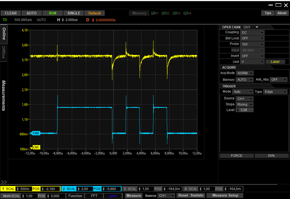
But for some reason I can't get it to work on the STMF411. Infact the clock isn't even working correctly as you can see on the oscilloscope.
Yellow is the Clock and Blue is MOSI. (Yellow is scaled to 500mv and Blue to 5v)
Maybe my configuration is wrong?
I hope someone could help me it and spot the mistake.
Thanks in advance!
#include "main.h"

#include <string.h>
#include <stdio.h>

//ioSpeedConfig
#define LOW_SPEED 0x00
#define MEDIUM_SPEED 0x01
#define FAST_SPEED 0x02
#define HIGH_SPEED 0x03
//ioPinConfig
#define INPUT_MODE 0x00
#define OUTPUT_MODE 0x01
#define ALTERNATIVE_MODE 0x02
#define ANALOG_MODE 0x03
//ioOtypeConfig
#define Push_Pull 0x00
#define Open_Drain 0x01
//ioPushPullConfig
#define NO_PULL 0x00
#define PULL_UP 0x01
#define PULL_DOWN 0x02

#define SET_PIN 1
#define RESET_PIN 0

#define AF0 0000 //system
#define AF1 0001 //(TIM1/TIM2)
#define AF2 0010 //(TIM3..5)
#define AF3 0011 //(TIM9..11)
#define AF4 0100 //(I2C1..3)
#define AF5 0101 //(SPI1..4)
#define AF6 0110 //(SPI3..5)
#define AF7 0111 //(USART1..2)
#define AF8 1000 //(USART6)
#define AF9 1001 //(I2C2..3)
#define AF10 1010 //(OTG_FS)
#define AF11 1011 //NOTHING?
#define AF12 1100 //(SDIO)
#define AF13 1101 //NOTHING?
#define AF14 1110 //NOTHING?
#define AF15 1111 //(EVENTOUT)

UART_HandleTypeDef huart2;

const uint8_t SPI_READ = 0x80;
const uint8_t PWR_MGMNT_1 = 0x6B;
const uint8_t PWR_RESET = 0x80;
const uint8_t WHO_AM_I = 0x75;

void SystemClock_Config(void);
static void MX_GPIO_Init(void);
static void MX_USART2_UART_Init(void);

void ioPinConfig(GPIO_TypeDef *portName, uint8_t pinNum, uint8_t configValue);
void ioPinSetReset(GPIO_TypeDef *portName, uint8_t pinNum, uint8_t pinState);
void ioPinPullConfig(GPIO_TypeDef *portName, uint8_t pinNum, uint8_t configValue);
void ioPinAlternateFunConfig(GPIO_TypeDef *portName, uint8_t pinNum, uint8_t configValue);
void ioPinOTypeConfig(GPIO_TypeDef *portName, uint8_t pinNum, uint8_t configValue);
void ioPinSetReset(GPIO_TypeDef *portName, uint8_t pinNum, uint8_t pinState);
uint8_t readRegister(SPI_TypeDef *spih, uint8_t subAddress);
void writeRegister(SPI_TypeDef *spih, uint8_t subAddress, uint8_t value);

void ioPinConfig(GPIO_TypeDef *portName, uint8_t pinNum, uint8_t configValue)
{
  portName->MODER = (portName->MODER & (~(0b11<<((2*pinNum))))) | (configValue << (2 * pinNum));
}

void ioPinSpeedConfig(GPIO_TypeDef *portName, uint8_t pinNum, uint8_t configValue)
{
  portName->OSPEEDR = (portName->OSPEEDR & (~(0b11<<((2*pinNum))))) | (configValue << (2 * pinNum));
}

void ioPinPullConfig(GPIO_TypeDef *portName, uint8_t pinNum, uint8_t configValue)
{
  portName->PUPDR = (portName->PUPDR & (~(0b11<<((2*pinNum))))) | (configValue << (2* pinNum));
}

void ioPinAlternateFunConfig(GPIO_TypeDef *portName, uint8_t pinNum, uint8_t configValue)
{
  if(pinNum < 8)
    portName->AFR[0] = (portName->AFR[0] & (~(0xF<<((4*pinNum))))) | (configValue << (4 * pinNum));
  else
    portName->AFR[1] = (portName->AFR[1] & (~(0xF<<((4*(pinNum-8)))))) | (configValue << (4 * (pinNum-8)));
}

void ioPinOTypeConfig(GPIO_TypeDef *portName, uint8_t pinNum, uint8_t configValue)
{
  portName->OTYPER = (portName->OTYPER & (~(0x01<<pinNum))) | configValue << pinNum;
}

void ioPinSetReset(GPIO_TypeDef *portName, uint8_t pinNum, uint8_t pinState)
{
  if(pinState == SET_PIN)
    portName->BSRR = (1 << pinNum);
  else
    portName->BSRR = (1 << (pinNum + 16));
}

uint8_t readRegister(SPI_TypeDef *spih, uint8_t subAddress)
{
  spih->DR = (subAddress | SPI_READ);
  while(!(spih->SR & (SPI_SR_TXE)));
  spih->DR = 0x00; //Send Dummy Data
  while(!(spih->SR & (SPI_SR_TXE)));
  while(!(spih->SR & (SPI_SR_RXNE)));
  while(spih->SR & (SPI_SR_BSY));
  return spih->DR;
}

void writeRegister(SPI_TypeDef *spih, uint8_t subAddress, uint8_t value)
{
  spih->DR = subAddress;
  while(!(spih->SR & (SPI_SR_TXE)));
  spih->DR = value;
  while(!(spih->SR & (SPI_SR_TXE)));
}


int main(void)
{

  HAL_Init();


  SystemClock_Config();

  MX_GPIO_Init();
  MX_USART2_UART_Init();

  ioPinConfig(GPIOB, 15, ALTERNATIVE_MODE); //MOSI
  ioPinConfig(GPIOB, 14, ALTERNATIVE_MODE); //MISO
  ioPinConfig(GPIOB, 13, ALTERNATIVE_MODE); //SCK

  ioPinOTypeConfig(GPIOB, 15, Push_Pull);
  ioPinOTypeConfig(GPIOB, 14, Push_Pull);
  ioPinOTypeConfig(GPIOB, 13, Push_Pull);

  ioPinPullConfig(GPIOB, 15, PULL_UP);
  ioPinPullConfig(GPIOB, 14, PULL_UP);
  ioPinPullConfig(GPIOB, 13, PULL_UP);

  ioPinAlternateFunConfig(GPIOB, 15, AF5);
  ioPinAlternateFunConfig(GPIOB, 14, AF5);
  ioPinAlternateFunConfig(GPIOB, 13, AF5);

  ioPinSpeedConfig(GPIOB, 15, HIGH_SPEED);
  ioPinSpeedConfig(GPIOB, 14, HIGH_SPEED);
  ioPinSpeedConfig(GPIOB, 13, HIGH_SPEED);
 //ENABLE SPI2 Clock
  RCC->APB1ENR |= RCC_APB1ENR_SPI2EN;
  SPI2->CR1 = 0x00;
  SPI2->CR1 |= SPI_CR1_SSM | SPI_CR1_SSI | 0x05 << 3 | SPI_CR1_MSTR | SPI_CR1_CPOL | SPI_CR1_CPHA;
  SPI2->CR2 = 0x00;
//Enable SPE
  SPI2->CR1 |= SPI_CR1_SPE;

  writeRegister(SPI2, PWR_MGMNT_1, PWR_RESET);
  writeRegister(SPI2, 0x1B, 0x18);

  char buffer[16];


  while (1)
  {
//read WhoAmI Register to check if the device is working
    uint8_t whoAmIData = readRegister(SPI2, WHO_AM_I);
    sprintf(buffer, "WhoAmI: %d\r\n", whoAmIData);
    HAL_UART_Transmit(&huart2, buffer, strlen(buffer), HAL_MAX_DELAY);
  }

}


void SystemClock_Config(void)
{
  RCC_OscInitTypeDef RCC_OscInitStruct = {0};
  RCC_ClkInitTypeDef RCC_ClkInitStruct = {0};


  __HAL_RCC_PWR_CLK_ENABLE();
  __HAL_PWR_VOLTAGESCALING_CONFIG(PWR_REGULATOR_VOLTAGE_SCALE1);

  RCC_OscInitStruct.OscillatorType = RCC_OSCILLATORTYPE_HSI;
  RCC_OscInitStruct.HSIState = RCC_HSI_ON;
  RCC_OscInitStruct.HSICalibrationValue = RCC_HSICALIBRATION_DEFAULT;
  RCC_OscInitStruct.PLL.PLLState = RCC_PLL_ON;
  RCC_OscInitStruct.PLL.PLLSource = RCC_PLLSOURCE_HSI;
  RCC_OscInitStruct.PLL.PLLM = 16;
  RCC_OscInitStruct.PLL.PLLN = 336;
  RCC_OscInitStruct.PLL.PLLP = RCC_PLLP_DIV4;
  RCC_OscInitStruct.PLL.PLLQ = 4;
  if (HAL_RCC_OscConfig(&RCC_OscInitStruct) != HAL_OK)
  {
    Error_Handler();
  }

  RCC_ClkInitStruct.ClockType = RCC_CLOCKTYPE_HCLK|RCC_CLOCKTYPE_SYSCLK
                              |RCC_CLOCKTYPE_PCLK1|RCC_CLOCKTYPE_PCLK2;
  RCC_ClkInitStruct.SYSCLKSource = RCC_SYSCLKSOURCE_PLLCLK;
  RCC_ClkInitStruct.AHBCLKDivider = RCC_SYSCLK_DIV1;
  RCC_ClkInitStruct.APB1CLKDivider = RCC_HCLK_DIV2;
  RCC_ClkInitStruct.APB2CLKDivider = RCC_HCLK_DIV1;

  if (HAL_RCC_ClockConfig(&RCC_ClkInitStruct, FLASH_LATENCY_2) != HAL_OK)
  {
    Error_Handler();
  }
}


static void MX_USART2_UART_Init(void)
{

  huart2.Instance = USART2;
  huart2.Init.BaudRate = 115200;
  huart2.Init.WordLength = UART_WORDLENGTH_8B;
  huart2.Init.StopBits = UART_STOPBITS_1;
  huart2.Init.Parity = UART_PARITY_NONE;
  huart2.Init.Mode = UART_MODE_TX_RX;
  huart2.Init.HwFlowCtl = UART_HWCONTROL_NONE;
  huart2.Init.OverSampling = UART_OVERSAMPLING_16;
  if (HAL_UART_Init(&huart2) != HAL_OK)
  {
    Error_Handler();
  }

}

static void MX_GPIO_Init(void)
{

  /* GPIO Ports Clock Enable */
  __HAL_RCC_GPIOC_CLK_ENABLE();
  __HAL_RCC_GPIOH_CLK_ENABLE();
  __HAL_RCC_GPIOA_CLK_ENABLE();
  __HAL_RCC_GPIOB_CLK_ENABLE();

}

void Error_Handler(void)
{

}
Solved! Go to Solution.
- Labels:
-
SPI
-
STM32F4 Series
Accepted Solutions
- Mark as New
- Bookmark
- Subscribe
- Mute
- Subscribe to RSS Feed
- Permalink
- Email to a Friend
- Report Inappropriate Content
2020-06-19 07:21 PM
RXNE gets set every time a byte comes in. For SPI, this happens every time you send a byte. For single byte transfers, you should:
- wait for TXE
- Set SPIx->DR = x
- Wait for RXNE
- Read SPIx->DR to clear RXNE
You're not doing this on every byte transfer.
- Mark as New
- Bookmark
- Subscribe
- Mute
- Subscribe to RSS Feed
- Permalink
- Email to a Friend
- Report Inappropriate Content
2020-06-19 04:06 AM
Is anything connected to that pin on the board? Try setting it to Out and toggle "manually" (you don't need to write code, you can do it in the debugger).
JW
- Mark as New
- Bookmark
- Subscribe
- Mute
- Subscribe to RSS Feed
- Permalink
- Email to a Friend
- Report Inappropriate Content
2020-06-19 04:47 AM
If I just set the connected Pins to Output and toggle them manually everything works as expected.
Furthermore the following code works fine as well.
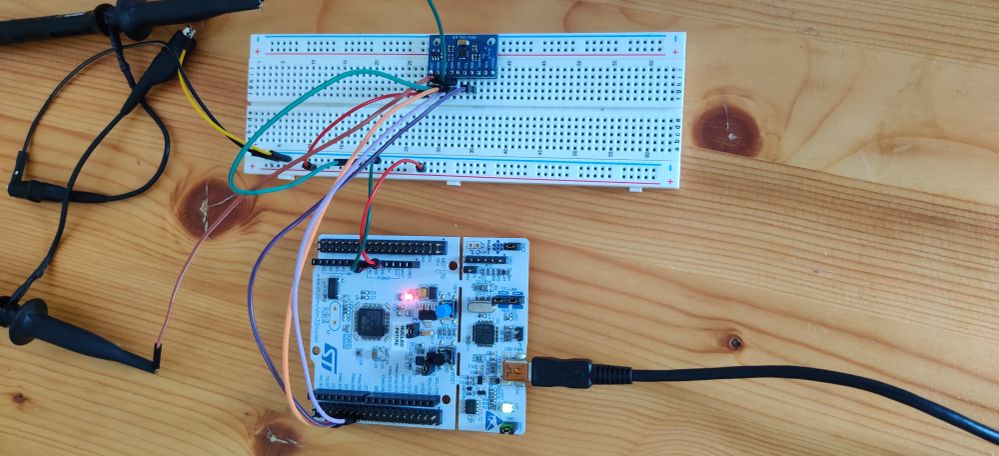
I also included a picture of the wiring. I Just connected the MPU6500 to the board nothing else.
  //Function definition is in the first post
  ioPinConfig(GPIOB, 15, OUTPUT_MODE);
  ioPinConfig(GPIOB, 13, OUTPUT_MODE);

  while (1)
  {
    ioPinSetReset(GPIOB, 15, SET_PIN);
    HAL_Delay(2);
    ioPinSetReset(GPIOB, 13, SET_PIN);
    HAL_Delay(2);
    ioPinSetReset(GPIOB, 13, RESET_PIN);
    ioPinSetReset(GPIOB, 15, RESET_PIN);
    HAL_Delay(2);

}- Mark as New
- Bookmark
- Subscribe
- Mute
- Subscribe to RSS Feed
- Permalink
- Email to a Friend
- Report Inappropriate Content
2020-06-19 05:57 AM
Reverting to original code, read out and check/post the SPI and relevant GPIO registers content.
When you'll get that code running, reduce length of those flying leads, making proper returns/grounds for the SPI signals (i.e. ground wires connected on both sides as close as possible to the signals), and reduce the GPIO drive.
JW
- Mark as New
- Bookmark
- Subscribe
- Mute
- Subscribe to RSS Feed
- Permalink
- Email to a Friend
- Report Inappropriate Content
2020-06-19 06:11 AM
Your code would be much clearer if you use the CMSIS register defines for your processor. Your defines for AFs should have a 'b'. Right now they are decimal numbers. Also, be careful with comments and #defines.
- Mark as New
- Bookmark
- Subscribe
- Mute
- Subscribe to RSS Feed
- Permalink
- Email to a Friend
- Report Inappropriate Content
2020-06-19 07:12 AM
#define AF5 0101 //(SPI1..4)

...

ioPinAlternateFunConfig(GPIOB, 15, AF5);
Here is at least one problem. In your code, AF5 = 65.
You should #include "stm32f4xx.h" and use the defines in there instead.
- Mark as New
- Bookmark
- Subscribe
- Mute
- Subscribe to RSS Feed
- Permalink
- Email to a Friend
- Report Inappropriate Content
2020-06-19 10:48 AM
Nice catch, TDK!
And a nasty C gotcha, too...
And, by pure coincidence, AF for PB15 and PB14 get set properly!
JW
PS. Easily discoverable by following my mantra, though...
- Mark as New
- Bookmark
- Subscribe
- Mute
- Subscribe to RSS Feed
- Permalink
- Email to a Friend
- Report Inappropriate Content
2020-06-19 12:01 PM
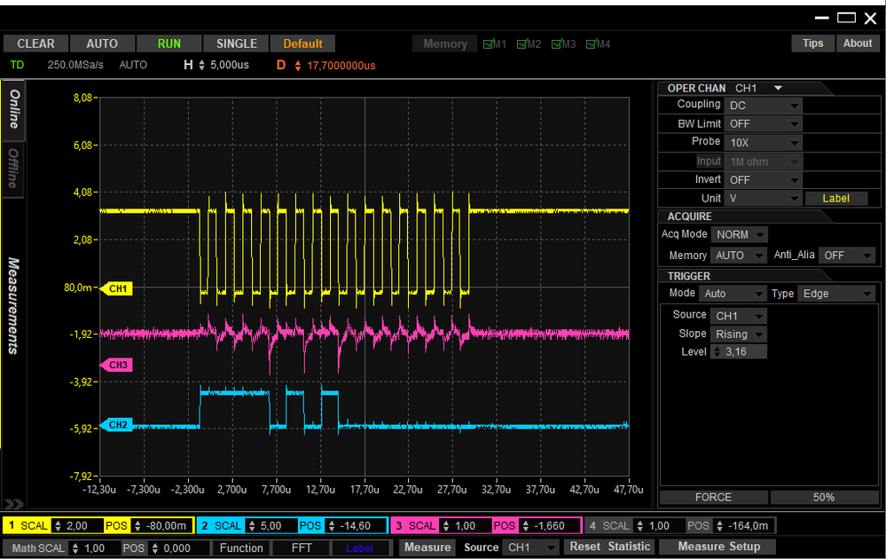
Yes that was the mistake, thank you very much.... After using the correct bits for AF5 the clock worked without a problem. The SPI sending now works as expected but sadly I don't receive anything.
Maybe someone knows something about the MPU6500 and why it's not working correctly?
I also tried to reduced the cable length and reduced the speed of the GPIO Pins but the response still looked likes in the following image of the oscilloscope.
Yellow: Clock, Blue: MOSI, Purple: MISO
- Mark as New
- Bookmark
- Subscribe
- Mute
- Subscribe to RSS Feed
- Permalink
- Email to a Friend
- Report Inappropriate Content
2020-06-19 12:02 PM
I look into the CMSIS Register thank you very much.
- Mark as New
- Bookmark
- Subscribe
- Mute
- Subscribe to RSS Feed
- Permalink
- Email to a Friend
- Report Inappropriate Content
2020-06-19 12:25 PM
> Maybe someone knows something about the MPU6500 and why it's not working correctly?
I don't see you toggling the CS pins anywhere. You need to do this so the chip knows where the transmission starts.
- Text not showing on new system - TouchGFX in STM32 MCUs TouchGFX and GUI
- What are the correct settings to run ADC at max speed on STM32H747I-DISCO? in STM32 MCUs products
- CubeMx clock resolver chooses the wrong USB clock frequency in STM32CubeMX (MCUs)
- Can't see stm 32 bootloader driver in device management after installing stm 32 cube programmer in STM32CubeProgrammer (MCUs)
- Readout external ADC by SPI doesn't work correctly in STM32CubeIDE (MCUs)


