- STMicroelectronics Community
- STM32 MCUs
- STM32 MCUs products
- Known issues with D-cache and FMC on STM32F7
- Subscribe to RSS Feed
- Mark Topic as New
- Mark Topic as Read
- Float this Topic for Current User
- Bookmark
- Subscribe
- Mute
- Printer Friendly Page
Known issues with D-cache and FMC on STM32F7
- Mark as New
- Bookmark
- Subscribe
- Mute
- Subscribe to RSS Feed
- Permalink
- Email to a Friend
- Report Inappropriate Content
2019-12-27 06:05 AM
Hi,
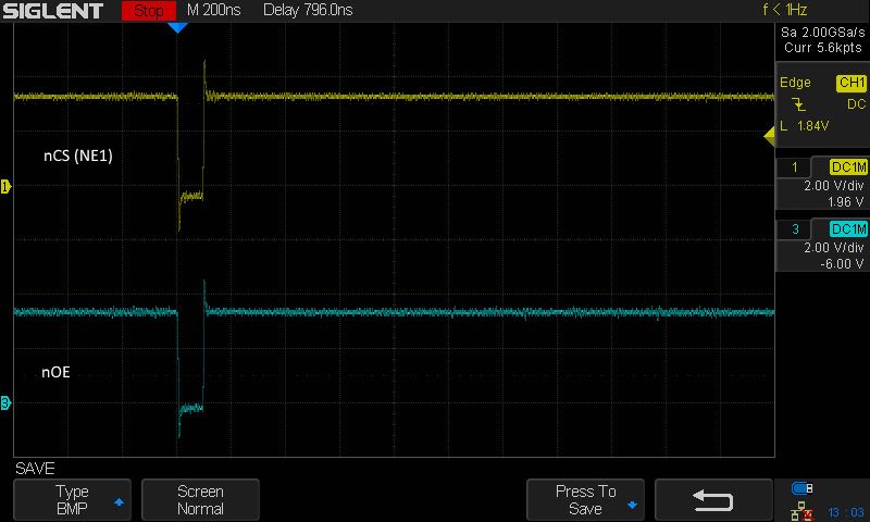
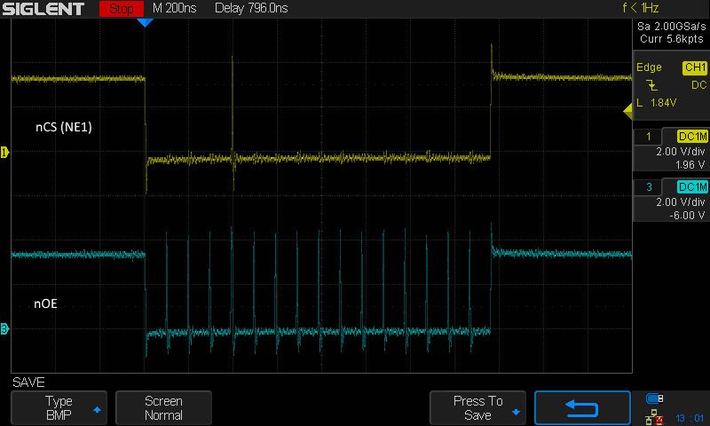
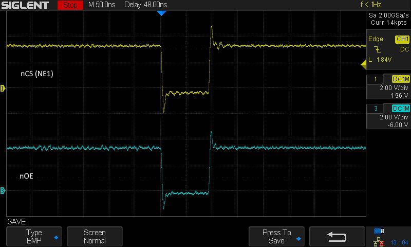
I'm using a STM32F765 clocked at 216MHz and when D-Cache is enabled it badly affects reads from a device connected via the external FMC address/data bus (NE1, 16 bit data, 10 bit address). The following pictures show the problem (note ringing is caused by non-optimum scope lead grounding)
D-Cache On:
D-Cache off (expected result & same time base as above):

I've checked the datasheets and errata but there is no mention of the issue I'm seeing. My multi-layer board is well decoupled, has ground & power planes and traces are short.
Has anyone come across this issue with D-Cache affecting FMC accesses ?
Thanks
Dave
- Labels:
-
FMC-FSMC
-
STM32F7 Series
- Mark as New
- Bookmark
- Subscribe
- Mute
- Subscribe to RSS Feed
- Permalink
- Email to a Friend
- Report Inappropriate Content
2019-12-27 06:19 AM
So what does "badly affects reads" actually mean?
Looks to be doing 16 operations for the cache-line.
Why not turn off caching for the FMC region if you don't want it buffered/cached?
Up vote any posts that you find helpful, it shows what's working..
- Mark as New
- Bookmark
- Subscribe
- Mute
- Subscribe to RSS Feed
- Permalink
- Email to a Friend
- Report Inappropriate Content
2019-12-27 06:27 AM
Clive
Perhaps 'badly affects' should be re-worded as 'unexpected effect' i.e. I wasn't expecting this behaviour.
I had considered turning off data caching when accessing this device but changing the cache enable setting has a fair bit of overhead. Is there a way of statically excluding the FMC region as your question alludes to ?
Dave
- Mark as New
- Bookmark
- Subscribe
- Mute
- Subscribe to RSS Feed
- Permalink
- Email to a Friend
- Report Inappropriate Content
2019-12-27 06:52 AM
You can config the MPU, likely several examples using a form similar to this
/**
  * @brief  Configure the MPU attributes as Normal Non Cacheable for SRAM1/2.
  * @note   The Base Address is 0x20010000 since this memory interface is the AXI.
  *         The Region Size is 512KB, it is related to SRAM1 and SRAM2  memory size.
  * @param  None
  * @retval None
  */
static void MPU_Config(void)
{
  MPU_Region_InitTypeDef MPU_InitStruct;

  /* Disable the MPU */
  HAL_MPU_Disable();

  /* Configure the MPU as Normal Non Cacheable for the SRAM1 and SRAM2 */
  MPU_InitStruct.Enable = MPU_REGION_ENABLE;
  MPU_InitStruct.BaseAddress = 0x20020000; // <<<< Change to FMC base
  MPU_InitStruct.Size = MPU_REGION_SIZE_512KB;
  MPU_InitStruct.AccessPermission = MPU_REGION_FULL_ACCESS;
  MPU_InitStruct.IsBufferable = MPU_ACCESS_NOT_BUFFERABLE;
  MPU_InitStruct.IsCacheable = MPU_ACCESS_NOT_CACHEABLE;
  MPU_InitStruct.IsShareable = MPU_ACCESS_SHAREABLE;
  MPU_InitStruct.Number = MPU_REGION_NUMBER1;
  MPU_InitStruct.TypeExtField = MPU_TEX_LEVEL1;
  MPU_InitStruct.SubRegionDisable = 0x00;
  MPU_InitStruct.DisableExec = MPU_INSTRUCTION_ACCESS_ENABLE;

  HAL_MPU_ConfigRegion(&MPU_InitStruct);

  /* Enable the MPU */
  HAL_MPU_Enable(MPU_PRIVILEGED_DEFAULT);
}Up vote any posts that you find helpful, it shows what's working..
- Mark as New
- Bookmark
- Subscribe
- Mute
- Subscribe to RSS Feed
- Permalink
- Email to a Friend
- Report Inappropriate Content
2019-12-27 07:02 AM
Many thanks Clive - I had the MPU disabled so I'll have a play to see the effect of this.
Dave
- Mark as New
- Bookmark
- Subscribe
- Mute
- Subscribe to RSS Feed
- Permalink
- Email to a Friend
- Report Inappropriate Content
2019-12-27 07:48 AM
There are two solutions.
Disable caching for a memory region in the MPU. The MPU is documented in the programming manual, not in the reference manual.
MPU->RBAR = ((uint32_t)0x60000000) | MPU_RBAR_VALID_Msk; // using region slot 0, FMC bank 0
MPU->RASR =
	MPU_RASR_XN_Msk            | // 1: Instruction fetches disabled
	(3u << MPU_RASR_AP_Pos)    | // Full access
	(19u << MPU_RASR_SIZE_Pos) | // 1 MB
	MPU_RASR_ENABLE_Msk        |
	0; // TEX,C,B,S are 0 meaning strongly ordered, this is the safest thing
This is more or less the same as what @Community member recommends, just avoiding HAL.
The size field is the base 2 logarithm of the size of the region - 1 (1MB = 2^20, so MPU_RASR_SIZE=20-1).
Remap the device into the 0xA0000000 - 0xDFFFFFFF range.
Address space above 0xA0000000 is treated as device memory, not cached by default (see AN4839). You can remap your device to 0xC0000000 by setting
SYSCFG->MEMRMP |= SYSCFG_MEMRMP_SWP_FMC_0;- Mark as New
- Bookmark
- Subscribe
- Mute
- Subscribe to RSS Feed
- Permalink
- Email to a Friend
- Report Inappropriate Content
2019-12-27 09:28 AM
Thanks berendi, your 2nd sugestion worked a treat!
I'd still like to know why data caching causes 16 reads for a single FMC read request if anyone has any insights.
Dave
- Mark as New
- Bookmark
- Subscribe
- Mute
- Subscribe to RSS Feed
- Permalink
- Email to a Friend
- Report Inappropriate Content
2019-12-27 09:05 PM
Cache cotrollers work that way.
The Cortex-M7 cache is organized into lines (sometimes called rows) that are 32 bytes long. A cache line is either filled or empty (invalid), there is no partially filled line. A read request from a cacheable memory area allocates a cache line and fills it with data. This works great with NAND and DRAM type memories that are organized in rows as well, e.g. if one memory cell of a DRAM is accessed, subsequent accesses to cells in the same row are faster, because the "row is opened", so the cache controller can read the rest of the line fast.
- Mark as New
- Bookmark
- Subscribe
- Mute
- Subscribe to RSS Feed
- Permalink
- Email to a Friend
- Report Inappropriate Content
2019-12-29 02:21 AM
Thanks berendi that makes sense and totally correlates with what I was seeing
- Mark as New
- Bookmark
- Subscribe
- Mute
- Subscribe to RSS Feed
- Permalink
- Email to a Friend
- Report Inappropriate Content
2021-01-23 09:35 AM
Although this post helped me there is an improvement to be made to the MPU configuration of Tesla which berendi did. The memory type has to be configured as Device or Strongly Ordered. (as berendi did, but I preferred the HAL implementation because it's better documented for the customer)
Please see the following post for more information on the TEX configuration and/or required memory barriers: https://community.st.com/s/question/0D50X00009hog4ISAQ/stm32f7h7-fmc-external-norflash-memory-why-it-works-only-by-use-dsb-command-for-cortexm7?t=1611421398835
- STM32F407 LWIP returning data to client in STM32 MCUs Embedded software
- Prevent speculative access using PRIVDEFENA in STM32 MCUs products
- Hard fault caused by unaligned access in STM32 MCUs products
- USBX CDC ACM on STM32F767 Nucleo board not working in STM32 MCUs Embedded software
- Nucleo-F767ZI MX_Device_HID example regeneration has multiple failures in STM32CubeMX (MCUs)

