- STMicroelectronics Community
- STM32 MCUs
- STM32 MCUs products
- How to use Output Compare for Timer 4 channel 1 fo...
- Subscribe to RSS Feed
- Mark Topic as New
- Mark Topic as Read
- Float this Topic for Current User
- Bookmark
- Subscribe
- Mute
- Printer Friendly Page
How to use Output Compare for Timer 4 channel 1 for STM32F407 Discovery demo board?
- Mark as New
- Bookmark
- Subscribe
- Mute
- Subscribe to RSS Feed
- Permalink
- Email to a Friend
- Report Inappropriate Content
2019-10-15 09:18 AM
/*This Program demonstrate the working of General Purpose Timer using Output Compare @1Hz Delay*/

//Toggle LED connected to TIM4_CH11 using Output compare mode @1Hz

#include "stm32f4xx.h" //Header File for STM32F4 device

//LED's connected to Timer and Channel
//PD12  - LED4: Green  - TIM4_CH1 used for Output compare
//PD13  - LED3: Orange - TIM4_CH2
//PD14  - LED5: Red    - TIM4_CH3
//PD15  - LED6: Blue   - TIM4_CH4

int main(void)
{

	//Enable AHB1ENR register in RCC to enable clock for GPIOD i.e. PD12
	RCC->AHB1ENR|=0x08;       //To enable GPIOD - RCC_AHB1ENR = 1000 = 0x08

	//Set the Direction or Mode register i.e. Input or Output , Here PD12 corresponds to 01
	GPIOD->MODER|=0x01000000;                  //0b 0000 0001 0000 0000 0000 0000 0000  0000

	//Configure Timer TIM4 Connected to APB1 ; @RCC_APB1ENR - Bit2 (TIM4EN)

	RCC->APB1ENR|=0x00000004;

/*If you see the register GPIOx_AFRL  it has 32 bit for 8 pins from 0 ---> 7.
You need to assign the PD12 PIN 12 the alternate function 2 (AF2).

Each pin has a bit field of 4 bits, so to write the AF2 to pin 12 you must write:

 0010 0000 0000 0000 0000 0000 0000 0000 0000 0000 0000  0000 0000  - This is for Pin 12 (AF2 hence 0010)

*/

	GPIOD->AFR[0]|=  ;

	//Prescaler setting for system clock =16000000/1600 =10000
	TIM4->PSC=1600-1;

	//Dividing prescaler = 10000 with Auto reload = 10000/10000 =1 sec
	TIM4->ARR=10000-1;

	//Toggle mode for Timer 4 match
	TIM4->CCMR1=0X30;

	//Capture register
	TIM4->CCR1=0;

	//Compare enable register enable
	TIM4->CCER|=1;

	//Clear the timer4 counter
	TIM4->CNT=0;

 	// Start the Timer4

	TIM4->CR1=1;

	while(1)
	{


	}

	return 0;
}
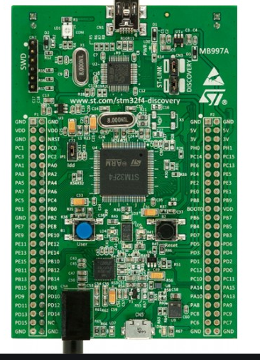
I am using STM32F4 discovery board. I want to use output compare mode for toggling LED.
So I decided to use Timer4 Channel 1. For discovery board the LED green is connected PD12 pin is connected to LED4: Green .
As per the datasheet, Timer 4 Channel 1 can be used as alternate function for LED green (PD12). So, for the alternate function configuration two registers are there.
AFR[0] (alternate function low register) and AFR[1] (alternate function high register).
How to configure this? What is the exact register value to be placed in this register?
As per my understanding for example to configure USART2 connected to (PA2) as AF7 (alternate function 7) .
The AF7 is the ID of the alternate function mode that you want to set at your PA2.
In fact, you know that the pin enabled for USART2_TX is the PA2 that means Port A - PIN 2
If you see the register GPIOx_AFRL it has 32 bit for 8 pins from 0 ---> 7. You need to assign the PIN2 the alternate function 7 (AF7).
Each pin has a bit field of 4 bits, so to write the AF7 to pin 2 you must write:
0x700. This is the value to be loaded into GPIOA->AFR[0]= 0x0700;
because 0x 7(pin2)0(pin1)0(pin0).
Now How to configure for Timer 4 Channel 1. My query is
to configure PD12 as AF2 I have to load bits as
0010 0000 0000 0000 0000 0000 0000 0000 0000 0000 0000 0000 0000 - This is for Pin 12 (PD12) as (AF2 hence 0010).
But, the register size has exceeded 32 bits. How to solve this? and what is the correct way to configure the alternate function for Timer 4 channel 1 for PD12 and AF2.
GPIOD->AFR[0]|= ? ;
Here I am attaching related pin descriptions.
Solved! Go to Solution.
- Labels:
-
STM32F4 Series
-
TIM
Accepted Solutions
- Mark as New
- Bookmark
- Subscribe
- Mute
- Subscribe to RSS Feed
- Permalink
- Email to a Friend
- Report Inappropriate Content
2019-10-15 09:43 AM
> //Set the Direction or Mode register i.e. Input or Output , Here PD12 corresponds to 01
> GPIOD->MODER|=0x01000000; //0b 0000 0001 0000 0000 0000 0000 0000 0000
No, you want to set to Alternate Function mode, that's 0b01 for the given field, ie.
GPIOD->MODER|=0x02000000;
For AFR, the field for pin 12 is in AFR[1]. AF for TIM4 is 2:
GPIOD->AFR[1] |= (2 << ( (12 - 😎 * 4)); // AFR[1] contains fields for pins 8..15 hence the offset 8; there are 4 bits per field hence the *4
JW
JW
- Mark as New
- Bookmark
- Subscribe
- Mute
- Subscribe to RSS Feed
- Permalink
- Email to a Friend
- Report Inappropriate Content
2019-10-15 11:24 AM
Great. Thanks for the analysis. It's working for me. Understood
- Mark as New
- Bookmark
- Subscribe
- Mute
- Subscribe to RSS Feed
- Permalink
- Email to a Friend
- Report Inappropriate Content
2019-10-15 11:35 AM
2 stands for AF2, which is the column in which you'll find TIM4_CH1 for PD12 in the Alternate function mapping table in 'F407 datasheet.
12 is for PD12; -8 is because AFR[1] (called AFRH in the RM) stores values starting from Px8, and not starting from Px0.
4 is the number of bits per one Px in AFR[x].
JW
- Mark as New
- Bookmark
- Subscribe
- Mute
- Subscribe to RSS Feed
- Permalink
- Email to a Friend
- Report Inappropriate Content
2019-10-16 09:40 AM
Hi, waclawek,
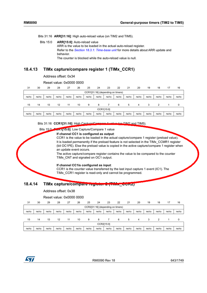
What is the use of CCRx Register for the timerx . How to use it and when to use it?
TIM4->CCR1=0; How does this effect?
Can you give an example for this register ?
- Mark as New
- Bookmark
- Subscribe
- Mute
- Subscribe to RSS Feed
- Permalink
- Email to a Friend
- Report Inappropriate Content
2019-10-21 06:49 AM
- 8 pulse pin outputs on the STM32F407 (Drive GPIO with basic timer?) in STM32 MCUs products
- On Block Diagram which BUS connects to the RCC in STM32 MCUs Boards and hardware tools
- I don't know what I can do after full chip erase in STM32 MCUs Boards and hardware tools
- STM32F407 discovery card debug error, Core is held in reset in STM32 MCUs products
- TIM Output compare on STM32F407 in STM32 MCUs products
