- STMicroelectronics Community
- STM32 MCUs
- STM32 MCUs products
- Can I use PH1 as GPIO if I config PH0 as HSE BYPAS...
- Subscribe to RSS Feed
- Mark Topic as New
- Mark Topic as Read
- Float this Topic for Current User
- Bookmark
- Subscribe
- Mute
- Printer Friendly Page
Can I use PH1 as GPIO if I config PH0 as HSE BYPASS Clock Source?
The same question on PC14, PC15 for LSE.
my chip is STM32H seriies. tks adv.
- Mark as New
- Bookmark
- Subscribe
- Mute
- Subscribe to RSS Feed
- Permalink
- Email to a Friend
- Report Inappropriate Content
2019-10-11 10:46 PM
- Mark as New
- Bookmark
- Subscribe
- Mute
- Subscribe to RSS Feed
- Permalink
- Email to a Friend
- Report Inappropriate Content
2019-10-12 11:32 AM
Yes.
10.3.14 Using the HSE or LSE oscillator pins as GPIOs
When the HSE or LSE oscillator is switched OFF (default state after reset), the related oscillator pins can be used as normal GPIOs.
When the HSE or LSE oscillator is switched ON (by setting the HSEON or LSEON bit in the RCC_CSR register) the oscillator takes control of its associated pins and the GPIO configuration of these pins has no effect.
When the oscillator is configured in a user external clock mode, only the OSC_IN or OSC32_IN pin is reserved for clock input and the OSC_OUT or OSC32_OUT pin can still be used as normal GPIO.
- Mark as New
- Bookmark
- Subscribe
- Mute
- Subscribe to RSS Feed
- Permalink
- Email to a Friend
- Report Inappropriate Content
2020-12-17 08:41 AM
Although it is mentioned that the PH1 is useable as a I/O, I do not succeed in doing so, on the standard configuration of a NucleoL053 where a 8Mhz clock signal is supplied from the ST-link part.
- Mark as New
- Bookmark
- Subscribe
- Mute
- Subscribe to RSS Feed
- Permalink
- Email to a Friend
- Report Inappropriate Content
2020-12-17 09:05 AM
+1
Concurring with your observation on the L0 series, definitely doesn't function with the STM32L072CZ used on the Murata LoRa device
Not usable as a GPIO w/BYPASS
Up vote any posts that you find helpful, it shows what's working..
- Mark as New
- Bookmark
- Subscribe
- Mute
- Subscribe to RSS Feed
- Permalink
- Email to a Friend
- Report Inappropriate Content
2020-12-17 09:35 AM
> Although it is mentioned that the PH1 is useable as a I/O
Where?
JW
- Mark as New
- Bookmark
- Subscribe
- Mute
- Subscribe to RSS Feed
- Permalink
- Email to a Friend
- Report Inappropriate Content
2020-12-17 10:10 AM
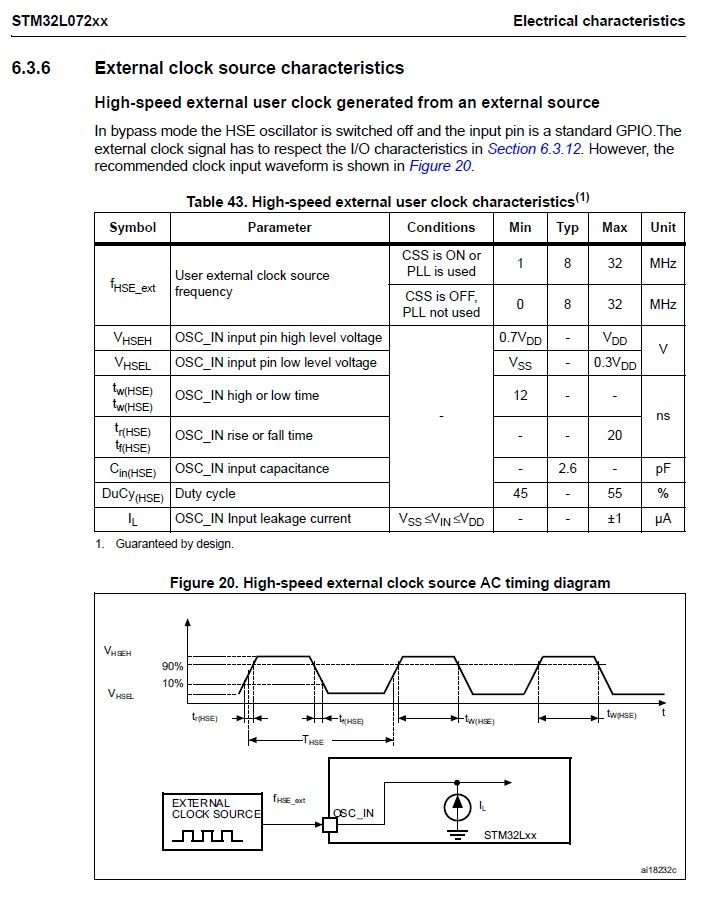
Now this admittedly is talking about OSC_IN, but the reasonable inference is that OSC_OUT should be uninvolved, and usable.
At a minimum this is poorly documented and misleading

Up vote any posts that you find helpful, it shows what's working..
- Mark as New
- Bookmark
- Subscribe
- Mute
- Subscribe to RSS Feed
- Permalink
- Email to a Friend
- Report Inappropriate Content
2020-12-17 10:13 AM
A secondary effect would be some potentially very undesirable behaviour out of the system boot loader..
Up vote any posts that you find helpful, it shows what's working..
- Mark as New
- Bookmark
- Subscribe
- Mute
- Subscribe to RSS Feed
- Permalink
- Email to a Friend
- Report Inappropriate Content
2020-12-17 10:16 AM
PC14/PC15 on STM32 implementations generally are within the low power domain, these pins have low drive expectations. Check data sheet on specifics
Up vote any posts that you find helpful, it shows what's working..
- Mark as New
- Bookmark
- Subscribe
- Mute
- Subscribe to RSS Feed
- Permalink
- Email to a Friend
- Report Inappropriate Content
2020-12-17 09:06 PM
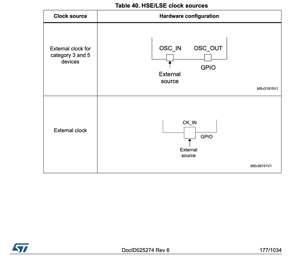
@Community member I was convinced that I had read it somewhere, but cannot retrieve it. Maybe it was the table 40 in the reference manual that was misleading me. But in the text it is written that the OSC_OUT must be left "hi-Z". Thanks for pointing this out.
- Mark as New
- Bookmark
- Subscribe
- Mute
- Subscribe to RSS Feed
- Permalink
- Email to a Friend
- Report Inappropriate Content
2023-07-28 09:54 AM
The initial reply to this post is correct. It works on the H7 series, see https://community.st.com/t5/stm32-mcu-products/in-clock-source-bypass-mode-can-we-use-the-osc-out-as-gpio/m-p/577976/highlight/true#M219627.
- STM32F769, generate a 2kHz clock on PC9. in STM32 MCUs products
- how to detect which line of code has modified the global variable (not debug mode) in STM32 MCUs Embedded software
- A Question regarding DMA controller trigger source in STM32 MCUs products
- How to get printf() to write to USART2? Using NUCLEO-F401RE and IAR. in STM32 MCUs Embedded software
- is stm32CubeIDE use C MISRA 2004 Compliance in STM32 MCUs Boards and hardware tools