- STMicroelectronics Community
- STM32 MCUs Software development tools
- STM32CubeMX (MCUs)
- FMC configuration for LCD interface
- Subscribe to RSS Feed
- Mark Topic as New
- Mark Topic as Read
- Float this Topic for Current User
- Bookmark
- Subscribe
- Mute
- Printer Friendly Page
FMC configuration for LCD interface
- Mark as New
- Bookmark
- Subscribe
- Mute
- Subscribe to RSS Feed
- Permalink
- Email to a Friend
- Report Inappropriate Content
2019-07-19 02:23 AM
Hello,
I am working on STM32F746ZG and I am trying to interfacing a display using FMC peripheral.
But actually I can't get it work... My display seems to receive some commands but I can't successfully send color.
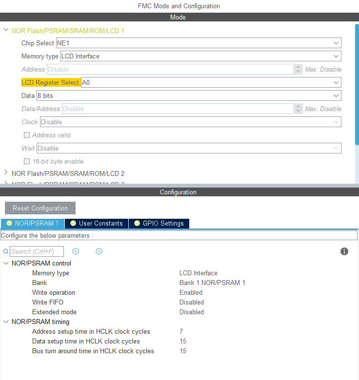
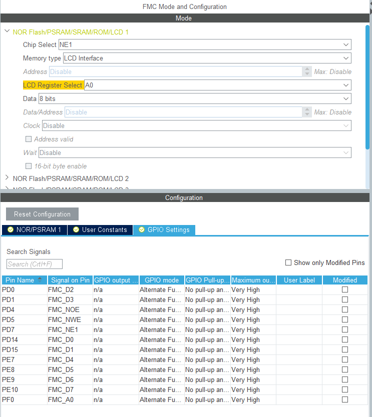
First of all I used CubeMX to configure my HW interface :
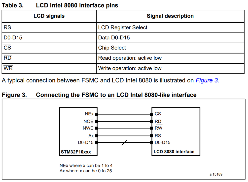
respecting A"N2790 TFT LCD interfacing with the high-density STM32F10xxx FSMC"
The generated code configured my FMC as :
SRAM_HandleTypeDef hsram1;

/**
  * @brief  Initializes LCD IO.
  */
void MX_FMC_Init(void)
{
/* FMC initialization function */

  /* USER CODE BEGIN FMC_Init 0 */

  /* USER CODE END FMC_Init 0 */

  FMC_NORSRAM_TimingTypeDef Timing = {0};

  /* USER CODE BEGIN FMC_Init 1 */

  /* USER CODE END FMC_Init 1 */

  /** Perform the SRAM1 memory initialization sequence
  */
  hsram1.Instance = FMC_NORSRAM_DEVICE;
  hsram1.Extended = FMC_NORSRAM_EXTENDED_DEVICE;
  /* hsram1.Init */
  hsram1.Init.NSBank = FMC_NORSRAM_BANK1;
  hsram1.Init.DataAddressMux = FMC_DATA_ADDRESS_MUX_DISABLE;
  hsram1.Init.MemoryType = FMC_MEMORY_TYPE_SRAM;
  hsram1.Init.MemoryDataWidth = FMC_NORSRAM_MEM_BUS_WIDTH_8;
  hsram1.Init.BurstAccessMode = FMC_BURST_ACCESS_MODE_DISABLE;
  hsram1.Init.WaitSignalPolarity = FMC_WAIT_SIGNAL_POLARITY_LOW;
  hsram1.Init.WaitSignalActive = FMC_WAIT_TIMING_BEFORE_WS;
  hsram1.Init.WriteOperation = FMC_WRITE_OPERATION_ENABLE;
  hsram1.Init.WaitSignal = FMC_WAIT_SIGNAL_DISABLE;
  hsram1.Init.ExtendedMode = FMC_EXTENDED_MODE_DISABLE;
  hsram1.Init.AsynchronousWait = FMC_ASYNCHRONOUS_WAIT_DISABLE;
  hsram1.Init.WriteBurst = FMC_WRITE_BURST_DISABLE;
  hsram1.Init.ContinuousClock = FMC_CONTINUOUS_CLOCK_SYNC_ONLY;
  hsram1.Init.WriteFifo = FMC_WRITE_FIFO_DISABLE;
  hsram1.Init.PageSize = FMC_PAGE_SIZE_NONE;
  /* Timing */
  Timing.AddressSetupTime = 6;
  Timing.AddressHoldTime = 15;
  Timing.DataSetupTime = 6;
  Timing.BusTurnAroundDuration = 5;
  Timing.CLKDivision = 16;
  Timing.DataLatency = 17;
  Timing.AccessMode = FMC_ACCESS_MODE_A;
  /* ExtTiming */

  if (HAL_SRAM_Init(&hsram1, &Timing, NULL) != HAL_OK)
  {
    Error_Handler( );
  }

  /* USER CODE BEGIN FMC_Init 2 */

  /* USER CODE END FMC_Init 2 */
}

/*  MSPInit/deInit Implementation */

static uint32_t FMC_Initialized = 0;

static void HAL_FMC_MspInit(void){
  /* USER CODE BEGIN FMC_MspInit 0 */

  /* USER CODE END FMC_MspInit 0 */
  GPIO_InitTypeDef GPIO_InitStruct ={0};
  if (FMC_Initialized) {
    return;
  }
  FMC_Initialized = 1;
  /* Peripheral clock enable */
  __HAL_RCC_FMC_CLK_ENABLE();

  /** FMC GPIO Configuration
  PF0   ------> FMC_A0
  PE7   ------> FMC_D4
  PE8   ------> FMC_D5
  PE9   ------> FMC_D6
  PE10   ------> FMC_D7
  PD14   ------> FMC_D0
  PD15   ------> FMC_D1
  PD0   ------> FMC_D2
  PD1   ------> FMC_D3
  PD4   ------> FMC_NOE
  PD5   ------> FMC_NWE
  PD7   ------> FMC_NE1
  */
  GPIO_InitStruct.Pin = GPIO_PIN_0;
  GPIO_InitStruct.Mode = GPIO_MODE_AF_PP;
  GPIO_InitStruct.Pull = GPIO_NOPULL;
  GPIO_InitStruct.Speed = GPIO_SPEED_FREQ_VERY_HIGH;
  GPIO_InitStruct.Alternate = GPIO_AF12_FMC;
  HAL_GPIO_Init(GPIOF, &GPIO_InitStruct);

  GPIO_InitStruct.Pin = GPIO_PIN_7|GPIO_PIN_8|GPIO_PIN_9|GPIO_PIN_10;
  GPIO_InitStruct.Mode = GPIO_MODE_AF_PP;
  GPIO_InitStruct.Pull = GPIO_NOPULL;
  GPIO_InitStruct.Speed = GPIO_SPEED_FREQ_VERY_HIGH;
  GPIO_InitStruct.Alternate = GPIO_AF12_FMC;
  HAL_GPIO_Init(GPIOE, &GPIO_InitStruct);

  GPIO_InitStruct.Pin = GPIO_PIN_14|GPIO_PIN_15|GPIO_PIN_0|GPIO_PIN_1
                          |GPIO_PIN_4|GPIO_PIN_5|GPIO_PIN_7;
  GPIO_InitStruct.Mode = GPIO_MODE_AF_PP;
  GPIO_InitStruct.Pull = GPIO_NOPULL;
  GPIO_InitStruct.Speed = GPIO_SPEED_FREQ_VERY_HIGH;
  GPIO_InitStruct.Alternate = GPIO_AF12_FMC;
  HAL_GPIO_Init(GPIOD, &GPIO_InitStruct);

  /* USER CODE BEGIN FMC_MspInit 1 */

  /* USER CODE END FMC_MspInit 1 */
}
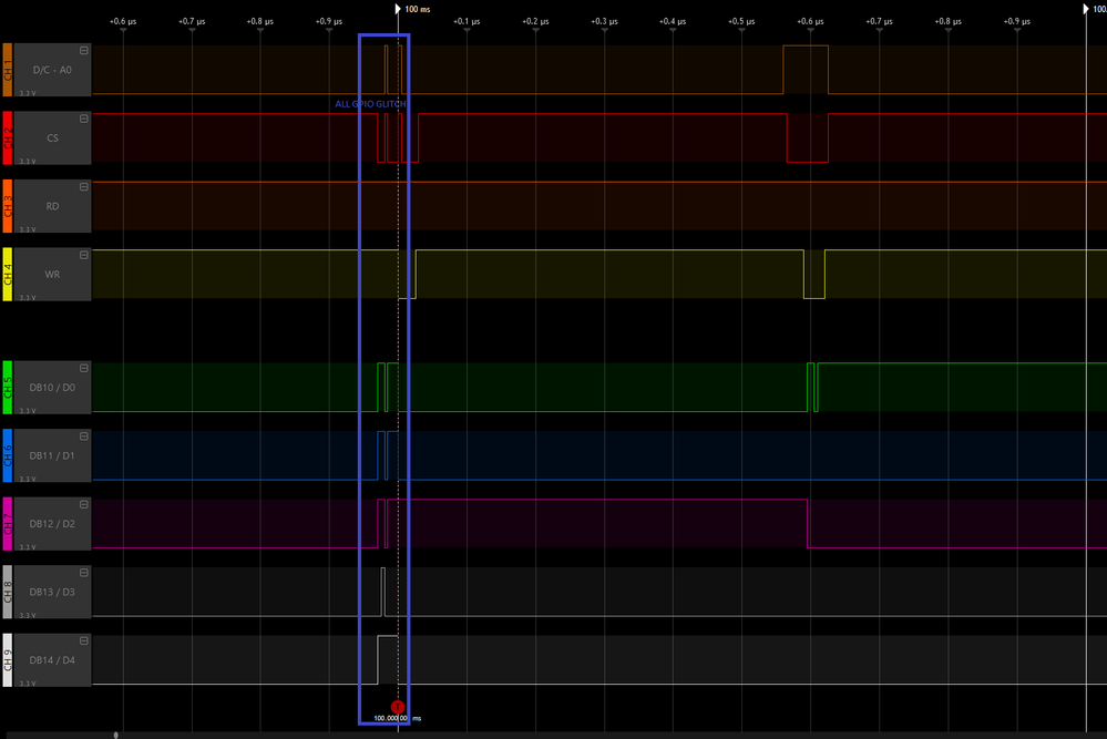
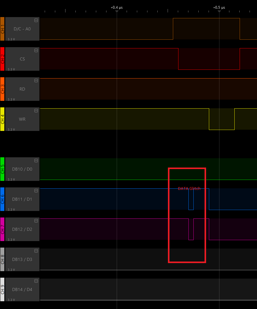
But its actually not works for some reasons. I measured each channel of my display interface and indeed I can see some glitch on the differents GPIO :
Why I got this glitch at first sent data ?. Which I got later on data :
Then, I tried to play with delay to works correctly and reduce delay between command and data :
Timing.AddressSetupTime = 1;
  Timing.AddressHoldTime = 1;
  Timing.DataSetupTime = 1;
  Timing.BusTurnAroundDuration = 5;
  Timing.CLKDivision = 1;
  Timing.DataLatency = 1;
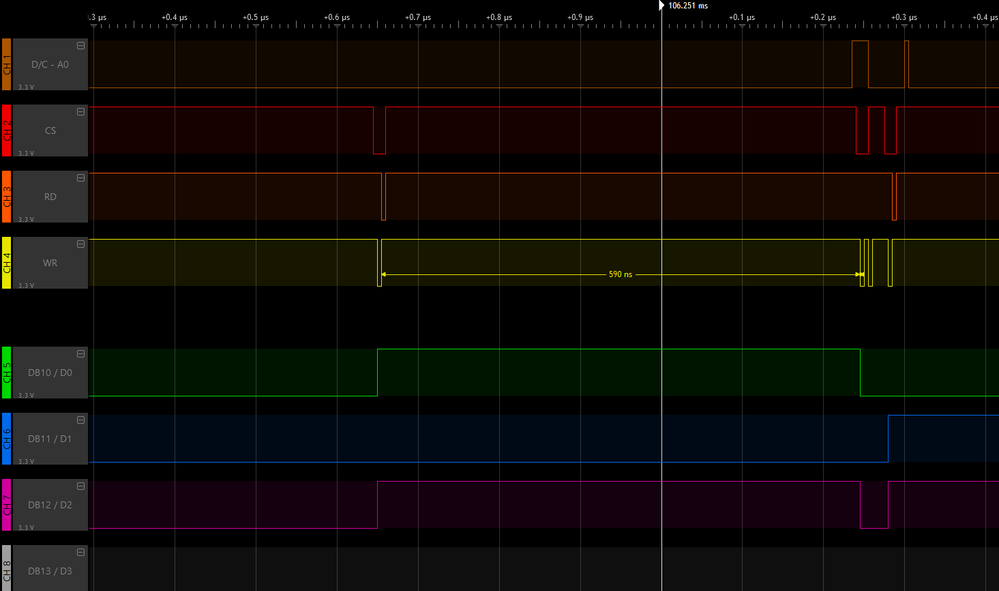
But the result is very strange ... :
Delay is exactly same. But read GPIO changes.... I don't even try to read. Why I got this result ?
Finally, I got some questions about FMC mode :
How can I swap between 8080 or 6800 mode ? (I can't see any mode A,B,C or D which write with NOE toggle)
Sry for this long post I a new with FMC peripheral.
I put question with Bold font to help you to find my questions =)
Thanks all !
Logan Gallois
- Labels:
-
FMC-FSMC
-
STM32CubeMX
-
STM32F7 Series
- Mark as New
- Bookmark
- Subscribe
- Mute
- Subscribe to RSS Feed
- Permalink
- Email to a Friend
- Report Inappropriate Content
2019-07-19 07:26 AM
Hello again,
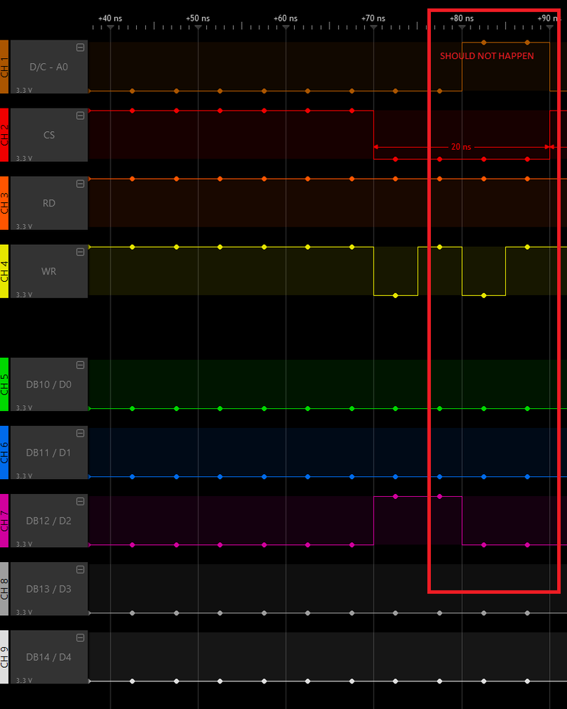
I successfully deleted the strange frame at start of transfer changing timing of AddressSetupTime to 0
Now my problem is that 2 write is done and Data/Sommand is changed. It shouldn't because I am trying to send only one command 0x04
I don't understand why I got this.
- Mark as New
- Bookmark
- Subscribe
- Mute
- Subscribe to RSS Feed
- Permalink
- Email to a Friend
- Report Inappropriate Content
2019-07-19 07:44 AM
Ok, well it's hard to tell without the context of how you're doing the writes, but it looks like it folded two writes, perhaps via the write buffering the Cortex-Mx.
Perhaps you should using some fencing commands/operations to separate the transactions?
The glitches described in your first post seem to be related to the data bus changing drive direction, or barrel shifting content, what happens prior to the rising edge of -WR surely should be irrelevant to the device that is latching on that edge?
You also don't specify what display/controller you are using, so it makes diagnosis rather hard, and whether you're actually looking at the right problem.
Up vote any posts that you find helpful, it shows what's working..
- Mark as New
- Bookmark
- Subscribe
- Mute
- Subscribe to RSS Feed
- Permalink
- Email to a Friend
- Report Inappropriate Content
2019-07-19 08:54 AM
Hi again,
Thanks for your answer
I should put also these configurations.
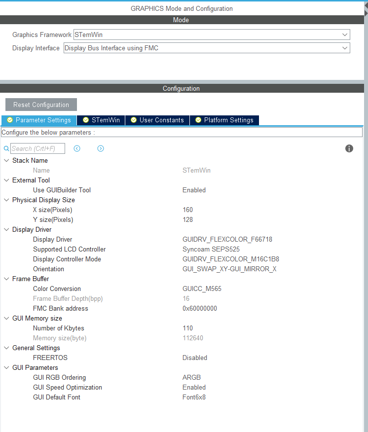
I am using an SEPS525 as Driver to control a display of 160*128 pixels.
I am using interface Intel 8080 with 8bits parallel for data actually.
first of all, I am just trying to write the register 0x04 (REDUCE_CURRENT) to 0x01 to power off my display.
Here is my code using to write the register and the data :
typedef struct
{
  __IO uint16_t REG;
  __IO uint16_t RAM;

}LCD_CONTROLLER_TypeDef;

/* The Bank address need to be entred by the USER */

#define FMC_BANK_BASE  ((uint32_t)       0x60000000  )
#define FMC_BANK       ((LCD_CONTROLLER_TypeDef *) FMC_BANK_BASE)

static void LcdWriteReg(U8 Data)
{
  FMC_BANK_WriteReg(Data);
}

static void LcdWriteData(U8 Data)
{
  FMC_BANK_WriteData(Data);
}

static void FMC_BANK_WriteReg(uint8_t Reg)
{
  FMC_BANK->REG = Reg;
}

static void FMC_BANK_WriteData(uint8_t Data)
{
  FMC_BANK->RAM = Data;
}

static void LCDController_Init(void)
{
// display off, analog reset
    LcdWriteReg(0x04); //At this moment, just try to send register command
    //LcdWriteData(0x01);
    osDelay(1);
}
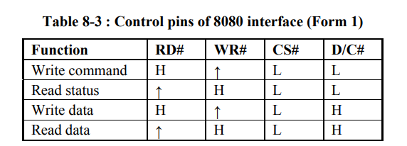
As my current mode is Intel 8080 transfer is done at WR rising edge as described :
So indeed, its not a real problem to have a "glitch" before the transfert (means rising up of WR).
My real problem is the second post when it seems to the bus to turn arround but I don't ask to read (I only write a register with LcdWriteReg(0x04);
- Mark as New
- Bookmark
- Subscribe
- Mute
- Subscribe to RSS Feed
- Permalink
- Email to a Friend
- Report Inappropriate Content
2021-08-23 02:30 PM
I think you declared the command and data pointers as uint16 causing 2 8 bit transfer.
- Issue with HR Timer PWM Frequency on STM32 in STM32CubeIDE (MCUs)
- Doubt related loading code and debugging with STM32 WL55JC controller in STM32CubeIDE (MCUs)
- Update Problem in STM32CubeMX (MCUs)
- STM32CubeIDE crashes - Problem: EXC_BAD_ACCESS (SIGABRT) in STM32CubeIDE (MCUs)
- STM32F446RET SPI Problem With CC1120 Device in STM32CubeIDE (MCUs)
