- STMicroelectronics Community
- STM32 MCUs
- STM32 MCUs Boards and hardware tools
- STM32L476VGT3 not booting on my pcb card
- Subscribe to RSS Feed
- Mark Topic as New
- Mark Topic as Read
- Float this Topic for Current User
- Bookmark
- Subscribe
- Mute
- Printer Friendly Page
STM32L476VGT3 not booting on my pcb card
- Mark as New
- Bookmark
- Subscribe
- Mute
- Subscribe to RSS Feed
- Permalink
- Email to a Friend
- Report Inappropriate Content
2019-06-21 01:39 AM
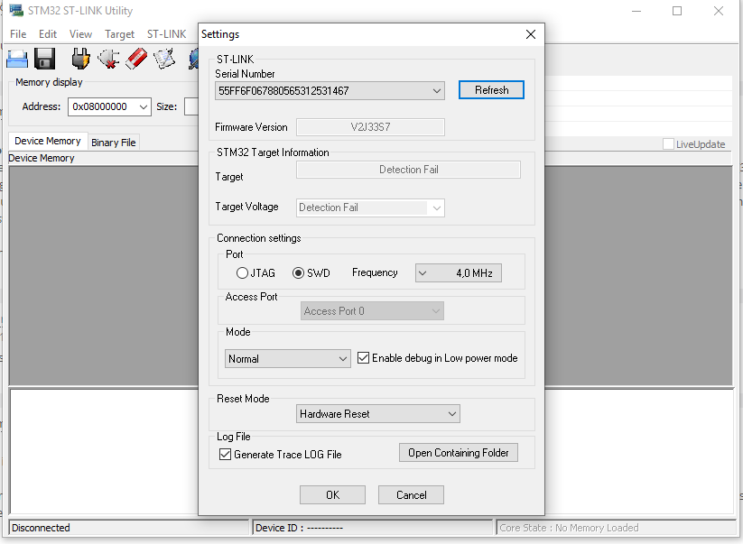
Hi, my mcu is not showing up in st-link v2 :(
Currently boot0 i low, 10k resistor to gnd.
All voltages are stable on vdd and no short circuit is detected.
Any tips or possible solutions to my problem?
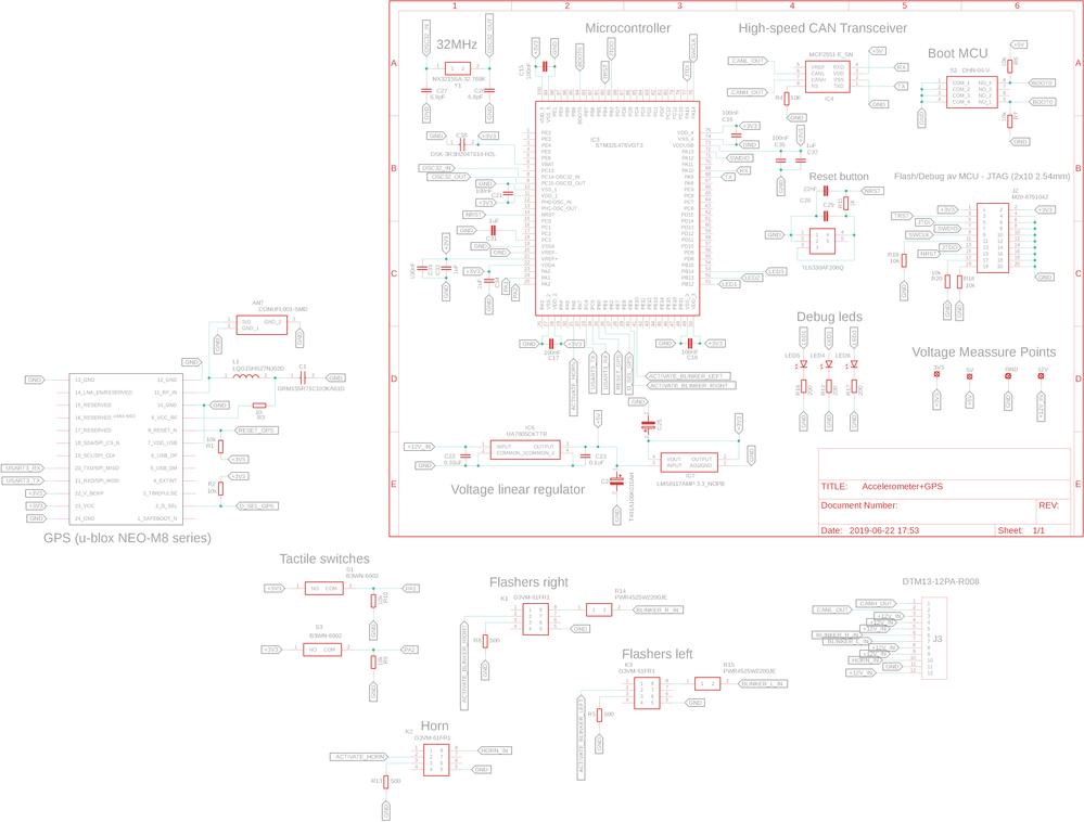
My schematic can be found here: https://gyazo.com/836f25b0cbac1570c4dc0bceeff82472
- Labels:
-
STM32L4 Series
- Mark as New
- Bookmark
- Subscribe
- Mute
- Subscribe to RSS Feed
- Permalink
- Email to a Friend
- Report Inappropriate Content
2019-06-21 01:57 AM
Nothing in the schematic immediately jumps out.
Pin 19 of the JTAG will have 3V from the ST-LINK on it.
What is the ST-LINK Utility or STM32 Cube Programmer reporting as a voltage on VTarget?
Check orientation of package on PCB
Check pin numbering
Check level on NRST
Up vote any posts that you find helpful, it shows what's working..
- Mark as New
- Bookmark
- Subscribe
- Mute
- Subscribe to RSS Feed
- Permalink
- Email to a Friend
- Report Inappropriate Content
2019-06-21 02:02 AM
Thanks for answer!
Pin 19 on jtag is nc? Should be 10k to gnd, or am I wrong here?
Nothing is showing up in ST-LINK Utility so cant see VTarget yet.
Orientation of package is ok.
What level should it be on NRST?
- Mark as New
- Bookmark
- Subscribe
- Mute
- Subscribe to RSS Feed
- Permalink
- Email to a Friend
- Report Inappropriate Content
2019-06-22 04:18 AM
Still haven't figured out whats wrong, anyone that might know?
- Mark as New
- Bookmark
- Subscribe
- Mute
- Subscribe to RSS Feed
- Permalink
- Email to a Friend
- Report Inappropriate Content
2019-06-22 08:41 AM
Schematic is a bit illegible, could do with being twice the resolution so the names are readable.
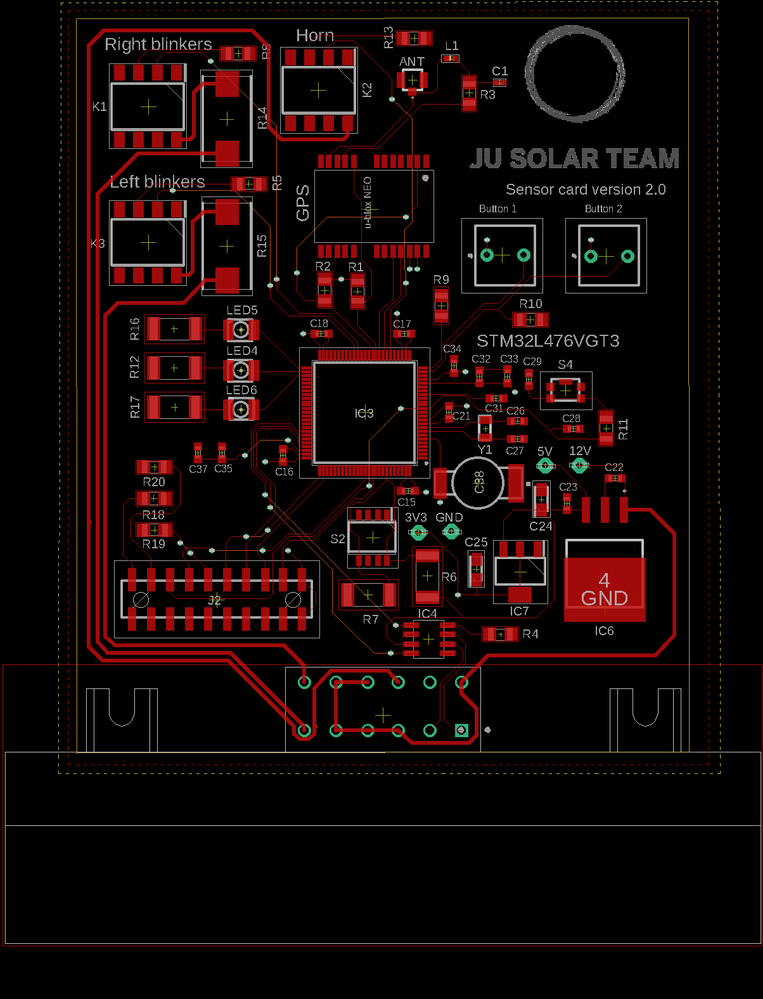
You have PCB image?
NRST should be high
Pin 19 is generally uncommitted, however Segger used it to output 5V and ST 3.3V, as a means to power a board. I'd leave the resistors off Pin 17 and Pin 19
ST-LINK should be able to report voltage even when it can't speak to the core.
Up vote any posts that you find helpful, it shows what's working..
- Mark as New
- Bookmark
- Subscribe
- Mute
- Subscribe to RSS Feed
- Permalink
- Email to a Friend
- Report Inappropriate Content
2019-06-22 08:58 AM
- Mark as New
- Bookmark
- Subscribe
- Mute
- Subscribe to RSS Feed
- Permalink
- Email to a Friend
- Report Inappropriate Content
2019-06-22 11:15 AM
Currently boot0 i low, 10k resistor to gnd.
That is not true. R6 and R7 forms a voltage divider. Also I don't understand why do You pull R6 up to 5V, when it should normally be pulled up to VDD (3,3 V). In this case it divides voltage to 5 V / 2 = 2,5 V, which is bad, because BOOT0 pin's high level is at minimum 0,77 * 3,3 V (VDD) = 2,541 V. So it turns out to be undetermined and close to high level, but it definitely is't low level, which is at maximum 0,17 * 3,3 V (VDD) = 0,561 V. Measure the voltage on BOOT0 and at least for testing connect it to GND by switching ON switch at pin NO_1 and all other switches OFF.
Minor comment.. Reset button circuit seems to be overly complicated.
- Mark as New
- Bookmark
- Subscribe
- Mute
- Subscribe to RSS Feed
- Permalink
- Email to a Friend
- Report Inappropriate Content
2019-06-22 11:18 AM
Understand your point, but i have cut the trace (5V 10k) so boot0 is only connected to 10k resistor to gnd. So that should not be any problem!
- Mark as New
- Bookmark
- Subscribe
- Mute
- Subscribe to RSS Feed
- Permalink
- Email to a Friend
- Report Inappropriate Content
2019-06-22 11:27 AM
OK, so BOOT0 is OK for now. By the way, if You didn't find it - AN4555 is pretty nice. 🙂
Maybe soldering problems? On LQFP packages pins can be measured with multimeter. Check all the power supply, BOOT0, NRST voltages on MCU pins. And also VSS voltages by measuring these against 3,3 V supply line.
- Mark as New
- Bookmark
- Subscribe
- Mute
- Subscribe to RSS Feed
- Permalink
- Email to a Friend
- Report Inappropriate Content
2019-06-23 12:33 AM
Have done some measurements, results:
VDD1: 3.29V
VDD2: 3.29V
VDD3: 3.29V
VDD4: 3.29V
VDD5: 3.29V
BOOT0: 0V
NRST: 3.17V (1.45V with ST-Link v2 unpowered) (3.17V with power)
Still nothing showing up in ST-LINK..
- stm32g0b1 Intern bootloader by FDCAN in STM32 MCUs Embedded software
- What am i not setting up right with dualbooting an STM32G474VET? in STM32 MCUs products
- Boot to RAM from SD card on STM32H7... in STM32 MCUs products
- boot loader - SD card in STM32 MCUs Embedded software
- STM32F407G RTC & SD Card(SPI) Not working simultaneously in STM32CubeMX (MCUs)


