- STMicroelectronics Community
- STM32 MCUs
- STM32 MCUs products
- DMA events from TIM1 - One Stream with 3 channels?
- Subscribe to RSS Feed
- Mark Topic as New
- Mark Topic as Read
- Float this Topic for Current User
- Bookmark
- Subscribe
- Mute
- Printer Friendly Page
DMA events from TIM1 - One Stream with 3 channels?
- Mark as New
- Bookmark
- Subscribe
- Mute
- Subscribe to RSS Feed
- Permalink
- Email to a Friend
- Report Inappropriate Content
2019-05-05 02:48 PM
I've been reading the STM32F427 and I can't confirm my understanding - so I'd like to ask.
I have data that I must push out a GPIO faster then should be serviced by an interrupt.
My intent is to use TIM1 - set a period - then set 3 output compares having each compare generate a DMA event.
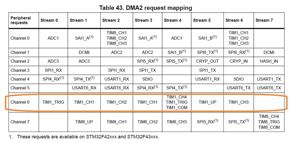
Looking at the Stream/Channel matrix I find Stream 6 DMA Channel 0 has TIM1_CH1, TIM1_CH2, TIM1_CH3, identified.
Does this imply that I can set up DMA Stream 6 to use DMA Channel 0 - AND - if I use CH1, CH2, CH3 of TIM1 for my compare that each DMA event from one of the TIM1 CHs will cause DMA Stream 6 to execute?
Any clarity in this matter is appreciated.
Thanks.
Joe
- Labels:
-
DMA
-
STM32F4 Series
-
TIM
- Mark as New
- Bookmark
- Subscribe
- Mute
- Subscribe to RSS Feed
- Permalink
- Email to a Friend
- Report Inappropriate Content
2019-05-05 03:02 PM
You're going to have to use Channel 6 across different Streams to separate the DMA transfers, otherwise you'll get one pattern buffer and you'll have to interleave the patterns as they will be occurring.
Up vote any posts that you find helpful, it shows what's working..
- Mark as New
- Bookmark
- Subscribe
- Mute
- Subscribe to RSS Feed
- Permalink
- Email to a Friend
- Report Inappropriate Content
2019-05-05 03:37 PM
I tried to keep my question simple but I think I muddied what I need to do.
I need to write to 3 separate GPIO ports for each Timer event (3 of them).
I believe what you explained is good for 1 GPIO but I have 3 which would require 9 Streams - and only DMA2 can to memory to memory giving 8 Streams.
So what I was hoping to do was to create my data in an array that properly interleaved them and have one DMA Stream 6 use DMA channel 0 which I am hoping will respond to each of the 3 TIM channel compare events then have DMA Stream 2 also use DMA Channel 0 and respond to the 3 TIM 8 events and finally have DMA Stream 1/Channel 6 AND Stream 3/Channel 7 AND Stream 4/Channel 7 provide the data to my third GPIO port.
I would have TIM8 linked to TIM1 so the timing on the 3 events (TIM1 and TIM8) should work for my 3 Stream output to the third GPIO.
I did not want to get this deep but this is what my understand is -- am I correct to proceed or I'm I totally lost?
Thanks in advance for any reply.
Joe
- Mark as New
- Bookmark
- Subscribe
- Mute
- Subscribe to RSS Feed
- Permalink
- Email to a Friend
- Report Inappropriate Content
2019-05-05 04:56 PM
I don't see you pulling that off.
Use the FMC/FSMC, create a 32-bit wide data bus, latch the 24-bits you want to drive externally.
Up vote any posts that you find helpful, it shows what's working..
- Mark as New
- Bookmark
- Subscribe
- Mute
- Subscribe to RSS Feed
- Permalink
- Email to a Friend
- Report Inappropriate Content
2019-05-05 05:13 PM
I'm actually trying to output 48 bits.
I am just testing 16 bit now (a single GPIO port) - polling - not interrupt or DMA to make sure I have the timer working properly.
The CCxIF flags in the TIM1 SR register are being set when the compare fires but I am unable to write to the SR register and reset the flags.
Am I missing something on polling - resetting the SR flags?
Thanks.
- LPBAM I2C data buffer using NUCLEO-U575ZI-Q in STM32 MCUs products
- AcousticBF (Beamforming) generates only noise. in STM32 MCUs Embedded software
- DMA1 Stream7 DMA2 Stream7 in STM32 MCUs products
- Generate single pulses based on capture event in STM32 MCUs products
- Missing or unaligned sample in buffer when using ADC and DMA in STM32 MCUs products
