- STMicroelectronics Community
- STM32 MCUs
- STM32 MCUs products
- Can't get TIM4 TOGO to start ADC3 conversions on S...
- Subscribe to RSS Feed
- Mark Topic as New
- Mark Topic as Read
- Float this Topic for Current User
- Bookmark
- Subscribe
- Mute
- Printer Friendly Page
Can't get TIM4 TOGO to start ADC3 conversions on STM32F7DISCOVERY board.
- Mark as New
- Bookmark
- Subscribe
- Mute
- Subscribe to RSS Feed
- Permalink
- Email to a Friend
- Report Inappropriate Content
2019-01-07 10:46 AM
I'm trying to get TIM4_TOGO output to start conversions on ADC3 on a STM32F7 DISCOVERY board.
I've attached main.c. I use a GPIO output toggle with oscilloscope to detect code execution and timing. I can see the toggle from the TIM interrupt handler, with the correct timing I'm after. I don't see any toggle from the ADC Handler unless I use software start from the main infinite loop, but this is not from the timer. I've been looking at this for a few days and haven't made any progress, please help!
(Yes, I have other things going on in the code, including an OS for a GUI on an LCD, but the TIM4 interrupt is working ok, so I believe that it is generating update events OK, and the A/D works when started by software. Just not sure how to connect the two via TIM4_TOGO).
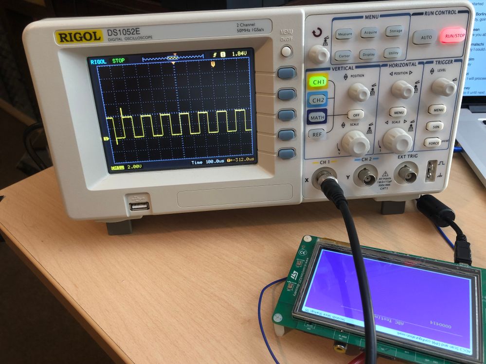
This first pic shows the output from the GPIO pin that is toggled from the TIM4 Interrupt handler. This is working perfectly. Not the timebase on scope is 100uS/div, and the toggle edges are a bit shorter than this. This is the rate I want to start ADC3 conversions.
When I check the ADC Interrupt by toggling the pin, which should be triggered by the timer and subsequent completion of the conversion at the same rate as the timer update, I don't get anything.
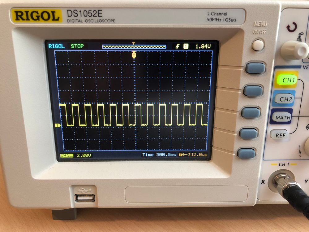
When testing the ADC3 by using the ADC software start in my infinite loop, I do get the toggle at the much lower frequency, which shows that the ADC Interrupt Handler is working at the end of conversions. (Note the timebase is now 500 ms!
Why is the TIM4_TOGO not causing an ADC3 trigger/conversion to start?
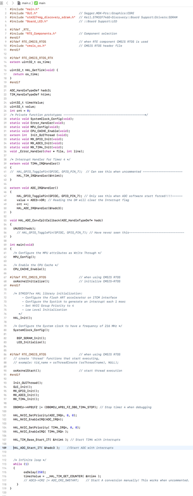
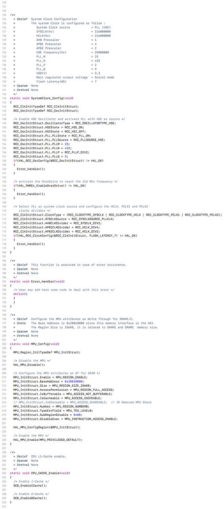
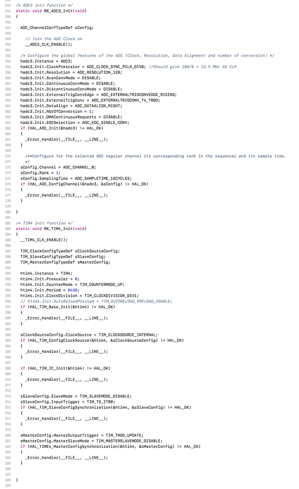
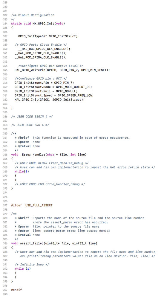
The main.c is attached, and below are images of my code with syntax color formatting and line numbers:
Any help greatly appreciated, I'm starting to pull my hair out!
Solved! Go to Solution.
- Labels:
-
ADC
-
STM32F7 Series
-
TIM
Accepted Solutions
- Mark as New
- Bookmark
- Subscribe
- Mute
- Subscribe to RSS Feed
- Permalink
- Email to a Friend
- Report Inappropriate Content
2019-01-11 03:05 AM
I think I've found the answer. I'm posting it here for anyone that is suffering from the same problems. Check the STM32F746 errata sheet.
"System 2.2.1 Missed ADC triggers from TIM1/TIM8, TIM2/TIM5/TIM4/TIM6/TRGO or TGRO2 event
Description The ADC external triggers for regular and injected channels by the TIM1, TIM8, TIM2, TIM5, TIM4 and TIM6 TRGO or TRGO2 events are missed at the following conditions: • Prescaler enabled on the PCLK2 clock. • TIMxCLK = 2xADCCLK and the master mode selection (MMS or MMS2 bits in the TIMx_CR2 timer register) as reset, update, or compare pulse configuration. • TIMxCLK = 4xADCCLK.
Workarounds • For TIM1 and TIM8 TRGO or TRGO 2 events: select the trigger detection on both the rising and falling edges. The EXTEN[1:0] or JEXTEN[1:0] bits must be set to 0x11 in the ADC_CR2 register. • For TIM2/TIM4/TIM5/TIM6/ TRGO or TGRO2 events: enable the DAC peripheral clock in the RCC_APB1ENR register."
- Mark as New
- Bookmark
- Subscribe
- Mute
- Subscribe to RSS Feed
- Permalink
- Email to a Friend
- Report Inappropriate Content
2019-01-07 11:35 AM
If you clear the interrupt in the primary IRQ Handler entry point it will never handed down to the callback.
Check if the ADC is flagging an overrun error.
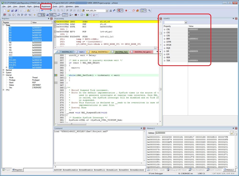
Avoid parking a Debugger Peripheral Viewer over the ADC.
Up vote any posts that you find helpful, it shows what's working..
- Mark as New
- Bookmark
- Subscribe
- Mute
- Subscribe to RSS Feed
- Permalink
- Email to a Friend
- Report Inappropriate Content
2019-01-07 11:47 AM
If pinout allows, route the Timer trigger signal to an GPIO for monitoring, then wire jump to the ADC trigger input pin. This way, you can see what happen and also break the link and apply GND/VDD/GND manually to see if the ADC is running. Do you use DMA to collect each ADC conversion?
- Mark as New
- Bookmark
- Subscribe
- Mute
- Subscribe to RSS Feed
- Permalink
- Email to a Friend
- Report Inappropriate Content
2019-01-07 12:05 PM
Thanks for pointing out about the callback, good spot. The problem is that the ADC primary IRQ Handler is not entered at all!
No ADC Overrun Error detected.
Can you expand on your comment "Avoid parking a Debugger Peripheral Viewer over the ADC." What do you mean by this, that I am toggling a GPIO in the Handler?
- Mark as New
- Bookmark
- Subscribe
- Mute
- Subscribe to RSS Feed
- Permalink
- Email to a Friend
- Report Inappropriate Content
2019-01-07 12:11 PM
I'll try outputting the timer trigger signal out to a pin. I did have DMA set up for collection of the ADC conversions, but I commented out/removed all DMA code until I can get the ADC trigger working reliably. I will build up the code once I get the ADC triggering regularly to use multiple regular channels in discontinuous mode, and then add a DMA to store the results. But for now I just want the ADC to trigger/convert regularly on the timer TOGO, and the ADC Interrupt Handler to occur after each conversion. This will show me that the timer output is triggering the ADC to start conversion.
- Mark as New
- Bookmark
- Subscribe
- Mute
- Subscribe to RSS Feed
- Permalink
- Email to a Friend
- Report Inappropriate Content
2019-01-07 12:53 PM
The debugger is invasive, if you inspect the peripheral registers in the debugger it will clear statuses, etc.
Up vote any posts that you find helpful, it shows what's working..
- Mark as New
- Bookmark
- Subscribe
- Mute
- Subscribe to RSS Feed
- Permalink
- Email to a Friend
- Report Inappropriate Content
2019-01-08 02:33 AM
Thanks, I'll remove the debugger watches for peripheral registers!
- Mark as New
- Bookmark
- Subscribe
- Mute
- Subscribe to RSS Feed
- Permalink
- Email to a Friend
- Report Inappropriate Content
2019-01-11 03:05 AM
I think I've found the answer. I'm posting it here for anyone that is suffering from the same problems. Check the STM32F746 errata sheet.
"System 2.2.1 Missed ADC triggers from TIM1/TIM8, TIM2/TIM5/TIM4/TIM6/TRGO or TGRO2 event
Description The ADC external triggers for regular and injected channels by the TIM1, TIM8, TIM2, TIM5, TIM4 and TIM6 TRGO or TRGO2 events are missed at the following conditions: • Prescaler enabled on the PCLK2 clock. • TIMxCLK = 2xADCCLK and the master mode selection (MMS or MMS2 bits in the TIMx_CR2 timer register) as reset, update, or compare pulse configuration. • TIMxCLK = 4xADCCLK.
Workarounds • For TIM1 and TIM8 TRGO or TRGO 2 events: select the trigger detection on both the rising and falling edges. The EXTEN[1:0] or JEXTEN[1:0] bits must be set to 0x11 in the ADC_CR2 register. • For TIM2/TIM4/TIM5/TIM6/ TRGO or TGRO2 events: enable the DAC peripheral clock in the RCC_APB1ENR register."
- STM32G071 ADC sequencer in not fully configurable mode and ADC channels set run-time changing in STM32 MCUs products
- HAL_ADC_Start_DMA from HAL_ADC_ConvCpltCallback in STM32 MCUs Embedded software
- ADC Returning "0" zeros in STM32CubeIDE (MCUs)
- How to read ADC without DMA ????? in STM32 MCUs products
- STM32F401RE - ADC SMPRx 'sample time setting' in STM32 MCUs Boards and hardware tools
