- STMicroelectronics Community
- Product forums
- Power management
- Should a inductor be added between Cin and the dra...
- Subscribe to RSS Feed
- Mark Topic as New
- Mark Topic as Read
- Float this Topic for Current User
- Bookmark
- Subscribe
- Mute
- Printer Friendly Page
Should a inductor be added between Cin and the drain of MOS in the applicaion of Liner Voltage Regulator in L9779
- Mark as New
- Bookmark
- Subscribe
- Mute
- Subscribe to RSS Feed
- Permalink
- Email to a Friend
- Report Inappropriate Content
2018-11-05 12:42 AM
I've got a problem about the engine management IC——L9779. I would really appreciate that if you could help.
Here is the thing:
A Liner Voltage Regulator has been built on this chip, which could transit the voltage from 12V to 5V and 3.3V.
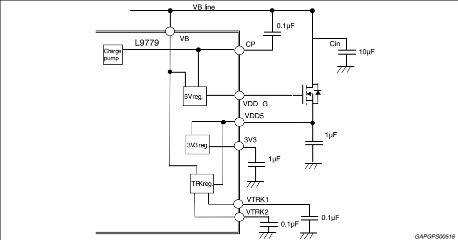
And this Regulator could work with dedicated external device. The typical application circuit are shown in the datasheet,
and I've shot it to the figure 1.
Figure 1 :typecal application circuit of L9779 voltage regulator.
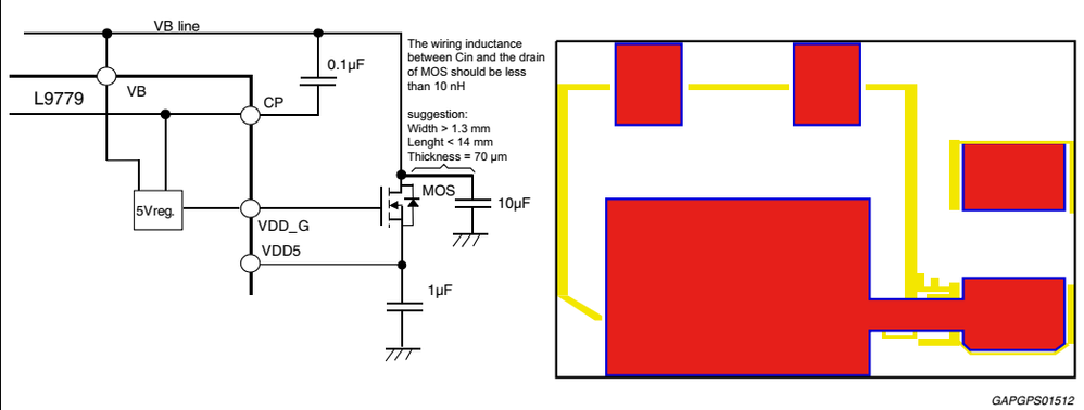
And there is a PCB design note which limited the PCB design rules, which is shown in figure 2.
Figure 2: PCB design rules for L9779 voltage regulator.
Based on this design limitation, the inductance between Cin and drain of MOS should be less than 10nH.
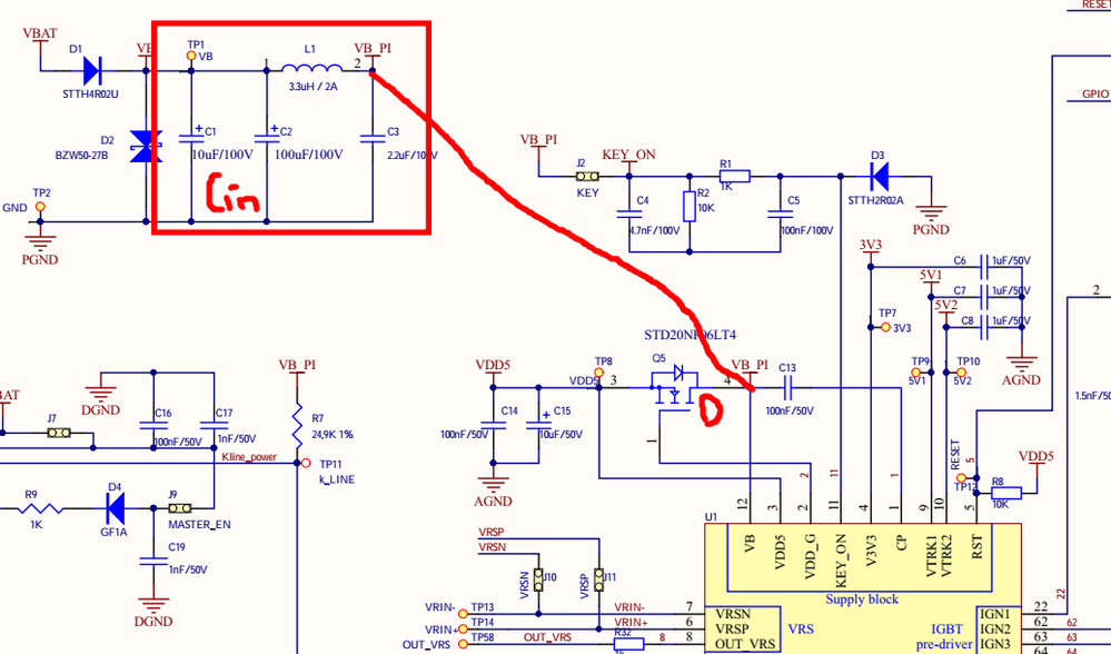
But here is the problem. I've refenced a application circuit from ST official website.(and I will attach it to this email)
This circuit is shown in figure3
Figure 3: A application circuit fron ST official website.
In this circuit a inductor is added between Cin and drain of MOS. I am confused about this design which is totally oppsite from the datasheet.
I want know whether this was a wrong application or not.
- Labels:
-
DC-DC Conversion
- Mark as New
- Bookmark
- Subscribe
- Mute
- Subscribe to RSS Feed
- Permalink
- Email to a Friend
- Report Inappropriate Content
2018-11-07 05:35 AM
Hello,
the statement of DS is correct and the circuit you are referring is in the imput side of VB. The C2-L1-C3 structure is a pi-greek filtering structure on the VB and is not related with the VDD5 loop. The DS statement means that the VDD5 regulation loop should be shrinked enough to avoid parasitic inductance in the reulation loop and L1 is not in this loop.
Please pay attention that the 3.3V is not a regualtor that should be used for any load. It is just an internal regualtor used to power the internal structure and cannot be used as an external regualtor.
Best regards
- Mark as New
- Bookmark
- Subscribe
- Mute
- Subscribe to RSS Feed
- Permalink
- Email to a Friend
- Report Inappropriate Content
2018-11-08 06:33 PM
First reply! Really thank you.
As you mentioned, the Pi-greek filtering module is not related with VDD5 loop. So there is not Cin in this circuit. Should the drain of MOS be closed to the C3,the right side capcitor of filtering ?
- Mark as New
- Bookmark
- Subscribe
- Mute
- Subscribe to RSS Feed
- Permalink
- Email to a Friend
- Report Inappropriate Content
2018-11-08 06:34 PM
First reply! Really thank you.
As you mentioned, the Pi-greek filtering module is not related with VDD5 loop. So there is not Cin in this circuit. Should the drain of MOS be closed to the C3,the right side capcitor of filtering ?
- Mark as New
- Bookmark
- Subscribe
- Mute
- Subscribe to RSS Feed
- Permalink
- Email to a Friend
- Report Inappropriate Content
2018-11-16 01:22 AM
Hello, Cin in this implementation is C15 that should be put closed to the pin.
- Mark as New
- Bookmark
- Subscribe
- Mute
- Subscribe to RSS Feed
- Permalink
- Email to a Friend
- Report Inappropriate Content
2019-11-30 12:13 PM
In the application circuit, 3.3u inductor is placed between VB and drian of MOS, not C3(Cin) and drian of MOS.
- STM32H747A in External SMPS supply mode not working. in STM32 MCUs Boards and hardware tools
- Problem with low inductor values and high current ripple and export to eDsim with ST8R00WPUR in eDesignSuite in Power management
- Problem with low inductor values and high current ripple with and export to eDsim with ST8R00WPUR in eDesignSuite in Other: software
- Getting wrong value from ADC - STM32G431KBT6 in STM32 MCUs products
- STM32WB55 Custom Board failing in STM32 MCUs Wireless


