- STMicroelectronics Community
- STM32 MCUs
- STM32 MCUs Boards and hardware tools
- Separate GND-plane for microcontroller crystal res...
- Subscribe to RSS Feed
- Mark Topic as New
- Mark Topic as Read
- Float this Topic for Current User
- Bookmark
- Subscribe
- Mute
- Printer Friendly Page
Separate GND-plane for microcontroller crystal resonator
- Mark as New
- Bookmark
- Subscribe
- Mute
- Subscribe to RSS Feed
- Permalink
- Email to a Friend
- Report Inappropriate Content
2018-10-24 09:44 AM
1. Background info
I'm designing a board for an STM32F767ZI microcontroller. This microcontroller has a primary oscillator for the `SYSCLK` (overall system clock) and a secondary oscillator for the `RTCCLK` (real-time clock).
I selected the following crystal for the primary oscillator:
> NX3225GD-8MHZ-EXS00A-CG04874 [DigiKey: 644-1391-1-ND]
And the following crystal for the secondary oscillator:
> NX3215SA-32.768KHZ-EXS00A-MU00525 [DigiKey: 644-1386-1-ND]
I selected the same crystals as those on the NUCLEO-F767ZI board from STMicroelectronics.
2. Recommendations from STMicroelectronics
The chip manufacturer recommends to provide a separate local GND-plane underneath each crystal. This GND-plane must be tied to the nearest GND-pin on the chip. I got that from Application Note AN2867:
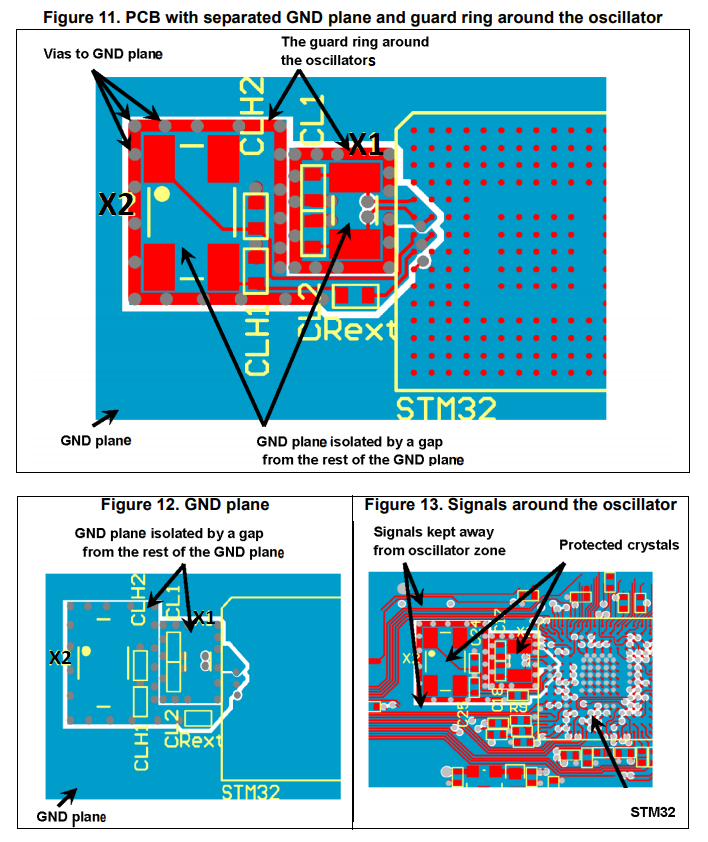
The following figure is from that document:
You can see two crystals on the figure: X1 and X2. Each has its own local GND-plane, separated by a gap from the overall board GND-plane.
3. How to apply?
I wonder how I can apply these recommendations on the STM32F767ZI chip:
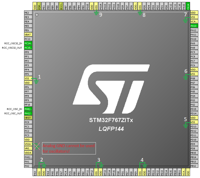
Please note the two oscillators on the left side: `RCC_OSC32` for the real-time clock and `RCC_OSC` for the general system clock. Also note the 9 GND pins (named `VSS`) on the chip.
Unfortunately, there is only one (!) GND pin on the left side of the chip. How can I properly apply the recommendations from STMicro? No matter what I try, I end up with one of the local GND-planes stretching out to reach a GND-pin far away ... probably not what STMicro had in mind.
Solved! Go to Solution.
- Labels:
-
STM32F7 Series
Accepted Solutions
- Mark as New
- Bookmark
- Subscribe
- Mute
- Subscribe to RSS Feed
- Permalink
- Email to a Friend
- Report Inappropriate Content
2018-10-24 10:33 AM
Perhaps look at the NUCLEO-144 gerbers to see how ST follows their own suggestions.
How many layers does your board have? Can you have the PF bank pins route east under the device?
A large ground fill under the QFP?
I think the end goal here is to avoid random current flows back to the regulators tracking under your oscillators and the wires connecting to the STM32. These should be low peak-to-peak signals, and you're trying to avoid interactions with signals banging rail-to-rail, or the less obvious return current paths as all the CMOS transistors switch state. The gaps don't impact the potential, just where the electrons want to go.
Up vote any posts that you find helpful, it shows what's working..
- Mark as New
- Bookmark
- Subscribe
- Mute
- Subscribe to RSS Feed
- Permalink
- Email to a Friend
- Report Inappropriate Content
2018-10-24 10:53 AM
Hi @Community member , I looked for the gerber files of this NUCLEO-F767ZI board. With a gerber viewer, I discovered that the general GND-plane runs under the oscillators as if they were no different from any other component. They definitely don't have their own local GND-plane.
Why is STMicro not following their own advice?
- Mark as New
- Bookmark
- Subscribe
- Mute
- Subscribe to RSS Feed
- Permalink
- Email to a Friend
- Report Inappropriate Content
2019-05-29 11:57 PM
In the FAQ about their ceramic resonators, Murata says:
- It is ideal to place land pattern of oscillation circuit symmetrically about the resonator.
- It is important to place the resonator close to the IC and make length of the tracks short.
- Do not run a ground plane under the ceramic resonator or under the tracks connecting the resonator and the IC.
My opinion: running a ground plane under the resonator or under the tracks connecting resonator and IC adds parasitic capacitance to the resonator, which changes resonator frequency slightly.
Reference: https://www.murata.com/en-eu/support/faqs/products/timingdevice/ceralock/mnt/cc0010
- Mark as New
- Bookmark
- Subscribe
- Mute
- Subscribe to RSS Feed
- Permalink
- Email to a Friend
- Report Inappropriate Content
2019-05-30 04:43 AM
Probably because the ST person didn't read their own app-notes. This whole thing of how to protect crystals from noise began in the 1960/70s (Bob Pease possibly ?) and I've been following it every since then so the app-note is correct, the designer was wrong. You can usually find a way to put the protective ground around the resonator in every case I've seen.
- Question on the RF-PLL calculations in STM32 MCUs Wireless
- STM32U5 sleep in STM32 MCUs Embedded software
- Audio stream with BLE in STM32 MCUs Wireless
- Issue with mbedTLS Handshake Failure When Using HyperRAM for FreeRTOS Heap in STM32 MCUs Security
- OV5640 JPEG Compression Issue When Storing Images on SD Card with STM32 in STM32 MCUs Embedded software

