Turn on suggestions
Auto-suggest helps you quickly narrow down your search results by suggesting possible matches as you type.
Showing results for
- STMicroelectronics Community
- STM32 MCUs
- STM32 MCUs products
- STM32F0 Discovery PF0 issue
Options
- Subscribe to RSS Feed
- Mark Topic as New
- Mark Topic as Read
- Float this Topic for Current User
- Bookmark
- Subscribe
- Mute
- Printer Friendly Page
STM32F0 Discovery PF0 issue
Options
- Mark as New
- Bookmark
- Subscribe
- Mute
- Subscribe to RSS Feed
- Permalink
- Email to a Friend
- Report Inappropriate Content
2013-08-27 09:46 AM
Posted on August 27, 2013 at 18:46
Hi there
According tohttp://www.st.com/st-web-ui/static/active/en/resource/technical/document/user_manual/DM00050135.pdf
PF0 is configured as GPIO.I didn't change any solder bridge settings but I cannot get access to PF0 as GPIO.PF1 works OK, PF0 doesn't.. the same configuration for both.I've tested it with three brand new boards.Any idea how to solve it?J. #rainbows-and-unicorns
3 REPLIES 3
Options
- Mark as New
- Bookmark
- Subscribe
- Mute
- Subscribe to RSS Feed
- Permalink
- Email to a Friend
- Report Inappropriate Content
2013-08-27 11:30 AM
Posted on August 27, 2013 at 20:30
I didn't change any solder bridge settings but I cannot get access to PF0 as GPIO.
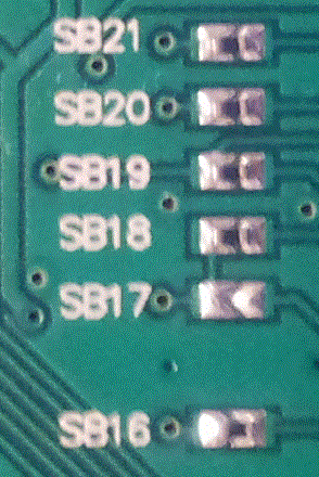
Why not? You'll need to remove SB18 to stop getting an 8 MHz signal from the ST-LINK's F103, and you'll need to make SB17 to get it too the external pin frame.
Tips, Buy me a coffee, or three.. PayPal Venmo
Up vote any posts that you find helpful, it shows what's working..
Up vote any posts that you find helpful, it shows what's working..
Options
- Mark as New
- Bookmark
- Subscribe
- Mute
- Subscribe to RSS Feed
- Permalink
- Email to a Friend
- Report Inappropriate Content
2013-08-27 02:47 PM
Posted on August 27, 2013 at 23:47That's from the manual:4.7.1 OSC clock supply
PF0 and PF1 can be used as GPIO or as HSE oscillator. By default these I/Os are
configured as GPIO, so SB16 and SB17 are closed, SB18 is open and R22, R23, C13 and
C14 are not populated.
I undestand SB18 is open by default.Edit:I've checked it - all SB 16 to 18 were open.
Options
- Mark as New
- Bookmark
- Subscribe
- Mute
- Subscribe to RSS Feed
- Permalink
- Email to a Friend
- Report Inappropriate Content
2013-08-27 05:39 PM
Posted on August 28, 2013 at 02:39  So, you'll probably want to stick a scope on the back of the board and see if you can get an 8 MHz clock. Then you'll want to look at how the pin is initialized. Make sure the GPIOF bank clock is enabled. Other STM32 parts needed some remapping of PDx pins, though there isn't any qualifier on the F0, but you do have to make sure that HSE is OFF/DISABLED.
That certainly deviates from the boards in my possession.
 So, you'll probably want to stick a scope on the back of the board and see if you can get an 8 MHz clock. Then you'll want to look at how the pin is initialized. Make sure the GPIOF bank clock is enabled. Other STM32 parts needed some remapping of PDx pins, though there isn't any qualifier on the F0, but you do have to make sure that HSE is OFF/DISABLED.
Tips, Buy me a coffee, or three.. PayPal Venmo
Up vote any posts that you find helpful, it shows what's working..
Up vote any posts that you find helpful, it shows what's working..
Related Content
- STM32H735-DK: SMPS vs LDO interesting observation in STM32 MCUs products
- Sensortile.boxpro Bluetooth in STM32 MCUs Wireless
- Problems with ST7789 LCD code (MCD Application Team) in STM32 MCUs Embedded software
- Cube says STM32F411 clock configuration is invalid, but processor still runs correctly in STM32CubeIDE (MCUs)
- USB FS Support in STM32 MCUs products