- STMicroelectronics Community
- STM32 MCUs
- STM32 MCUs products
- SPI issue. CLK Signal with a Level
- Subscribe to RSS Feed
- Mark Topic as New
- Mark Topic as Read
- Float this Topic for Current User
- Bookmark
- Subscribe
- Mute
- Printer Friendly Page
SPI issue. CLK Signal with a Level
- Mark as New
- Bookmark
- Subscribe
- Mute
- Subscribe to RSS Feed
- Permalink
- Email to a Friend
- Report Inappropriate Content
2013-11-25 07:08 AM
Hi everyone,
I am trying to implement the SPI1 by hardware in my STM32F407VGT6, I did everything and actually it seems to work. But I was trying to read the ID from my SPI device (which is a Flash Memory) and it doesn't work. So I used myoscilloscope
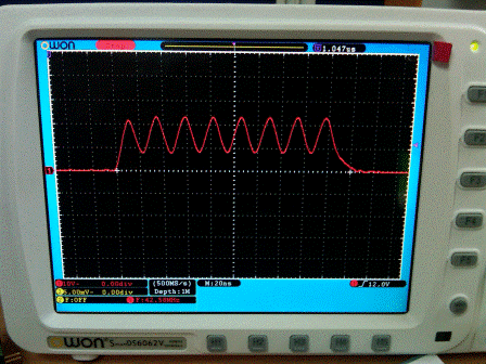
to watch the signal clock , and I got a CLK signal with a level on the bottom of it. Take a look, this picture shows my clk signal on my oscilloscope: 
As you can see the Signal has a level at the moment to start the clock signal. So, What do you think is happening with this?, and what are the hardware considerations to implement the SPI?, Should I use External Resistors?
This is my code://=================================================================
// SPI1 MEMORIA TRABAJO FLASH
//=================================================================
#define PORT_SPI1_SCLK GPIOA ///
#define PIN_SPI1_SCLK GPIO_Pin_5 ///
#define PORT_SPI1_SCLK_CLK RCC_AHB1Periph_GPIOA ///
#define PIN_SPI1_SCLK_Source GPIO_PinSource5 ///
#define PORT_SPI1_MISO GPIOA ///
#define PIN_SPI1_MISO GPIO_Pin_6 ///
#define PORT_SPI1_MISO_CLK RCC_AHB1Periph_GPIOA ///
#define PIN_SPI1_MISO_Source GPIO_PinSource6 ///
#define PORT_SPI1_MOSI GPIOA ////
#define PIN_SPI1_MOSI GPIO_Pin_7 ////
#define PORT_SPI1_MOSI_CLK RCC_AHB1Periph_GPIOA ///
#define PIN_SPI1_MOSI_Source GPIO_PinSource7 ///
#define PORT_SPI1_CS GPIOA ///
#define PIN_SPI1_CS GPIO_Pin_4 ///
#define PORT_SPI1_CS_CLK RCC_AHB1Periph_GPIOA ///
#define PORT_WM_RST GPIOC ////
#define PIN_WM_RST GPIO_Pin_4 ////
#define PORT_WM_RST_CLK RCC_AHB1Periph_GPIOC /
//=======================MACROS====================================
#define SPI1_WM SPI1
#define SPI1_WM_AF GPIO_AF_SPI1
#define SPI1_WM_CLK RCC_APB2Periph_SPI1
#define SPI1_WM_CLK_CMD RCC_APB2PeriphClockCmd
#define WM_CS_LOW GPIO_SetBits(PORT_SPI1_CS,PIN_SPI1_CS)
#define WM_CS_HIGH GPIO_ResetBits(PORT_SPI1_CS,PIN_SPI1_CS)
//=======================COMMANDS====================================
#define WREN 0x06 //Write Enable
#define WRDI 0x04 //Write Disable
#define RDID 0x9F //Read Identification
#define RDSR 0x05 //Read Status Register
#define READ 0x03 //Read Data Bytes
#define FAST_READ 0x0B //Read Data Bytes at Higher Speed
#define PW 0x0A //Page Write
#define PP 0x02 //Page Program
#define PE 0xDB //Page Erase
#define SE 0xD8 //Sector Erase
#define DP 0xB9 //Deep Power-Down
#define RDP 0xAB //Release from Deep Power-Downint main(void)
{
Spi1_Open();
while(1)
{
WorkMemory_ID();
Delayms(30);
}
}//====================READ STATUS=============================================
uint32_t WorkMemory_ID(void) { uint32_t ret = 0x00000000; int dat = 0x00; WM_CS_LOW; Spi1_Write(0x9F); dat = Spi1_Read(); ret = ( dat << 16) & 0x00FF0000; dat = Spi1_Read(); ret |= (dat << 8 ) & 0x0000FF00; dat = Spi1_Read(); ret |= (dat << 0 ) & 0x000000FF; WM_CS_HIGH; return ret; }//======================SPI INIT===========================================
void Spi1_Open(void)
{ GPIO_InitTypeDef GPIO_InitStruct;
SPI_InitTypeDef SPI_InitStruct;
SPI1_WM_CLK_CMD(SPI1_WM_CLK, ENABLE); //Enable Clock SPI1
GPIO_CLK_CMD(PORT_SPI1_SCLK_CLK, ENABLE); //Enable Clock SCKL
GPIO_CLK_CMD(PORT_SPI1_MISO_CLK, ENABLE); //Enable Clock MISO
GPIO_CLK_CMD(PORT_SPI1_MOSI_CLK, ENABLE); //Enable Clock MOSI
GPIO_CLK_CMD(PORT_SPI1_CS_CLK, ENABLE); //Enable Clock CS
//********** Configure the Chip Select************//
GPIO_InitStruct.GPIO_Pin = PIN_SPI1_CS;
GPIO_InitStruct.GPIO_Mode = GPIO_Mode_OUT;
GPIO_InitStruct.GPIO_OType = GPIO_OType_PP;
GPIO_InitStruct.GPIO_Speed = GPIO_Speed_100MHz;
GPIO_InitStruct.GPIO_PuPd = GPIO_PuPd_UP;
GPIO_Init(PORT_SPI1_CS, &GPIO_InitStruct);
WM_CS_HIGH;
//************* Configure the SCLK****************//
GPIO_InitStruct.GPIO_Pin = PIN_SPI1_SCLK;
GPIO_InitStruct.GPIO_Mode= GPIO_Mode_AF;
GPIO_InitStruct.GPIO_OType = GPIO_OType_PP;
GPIO_InitStruct.GPIO_PuPd = GPIO_PuPd_NOPULL;
GPIO_InitStruct.GPIO_Speed = GPIO_Speed_100MHz;
GPIO_Init(PORT_SPI1_SCLK, &GPIO_InitStruct);
//************* Configure the MISO****************//
GPIO_InitStruct.GPIO_Pin = PIN_SPI1_MISO;
GPIO_InitStruct.GPIO_Mode= GPIO_Mode_AF;
GPIO_InitStruct.GPIO_OType = GPIO_OType_OD;
GPIO_InitStruct.GPIO_Speed = GPIO_Speed_100MHz;
GPIO_Init(PORT_SPI1_MISO, &GPIO_InitStruct);
//************* Configure the MOSI****************//
GPIO_InitStruct.GPIO_Pin = PIN_SPI1_MOSI ;
GPIO_InitStruct.GPIO_Mode= GPIO_Mode_AF;
GPIO_InitStruct.GPIO_OType = GPIO_OType_PP;
GPIO_InitStruct.GPIO_Speed = GPIO_Speed_100MHz;
GPIO_Init(PORT_SPI1_MOSI, &GPIO_InitStruct);
//**************Alternate Function SPI**********************//
GPIO_PinAFConfig(PORT_SPI1_MOSI, PIN_SPI1_MOSI_Source, SPI1_WM_AF);
GPIO_PinAFConfig(PORT_SPI1_MISO, PIN_SPI1_MISO_Source, SPI1_WM_AF);
GPIO_PinAFConfig(PORT_SPI1_SCLK, PIN_SPI1_SCLK_Source, SPI1_WM_AF);
//************** SPI Config ***************************//
SPI_InitStruct.SPI_Direction = SPI_Direction_2Lines_FullDuplex; // set to full duplex mode, seperate MOSI and MISO lines
SPI_InitStruct.SPI_Mode = SPI_Mode_Master; // transmit in master mode, NSS pin has to be always high
SPI_InitStruct.SPI_DataSize = SPI_DataSize_8b; // one packet of data is 8 bits wide
SPI_InitStruct.SPI_CPOL = SPI_CPOL_Low; // clock is low when idle
SPI_InitStruct.SPI_CPHA = SPI_CPHA_1Edge; // data sampled at first edge
SPI_InitStruct.SPI_NSS = SPI_NSS_Soft;// | SPI_NSSInternalSoft_Set; // set the NSS management to internal and pull internal NSS high
SPI_InitStruct.SPI_BaudRatePrescaler = SPI_BaudRatePrescaler_8; // SPI frequency is APB2 frequency / 4
SPI_InitStruct.SPI_FirstBit = SPI_FirstBit_MSB;// data is transmitted MSB first
SPI_Init(SPI1_WM, &SPI_InitStruct);
SPI_Cmd(SPI1_WM, ENABLE); // enable SPI1
}- Labels:
-
SPI
- Mark as New
- Bookmark
- Subscribe
- Mute
- Subscribe to RSS Feed
- Permalink
- Email to a Friend
- Report Inappropriate Content
2013-11-25 07:54 AM
Provide a circuit diagram.
There looks to be some confusion about what a HIGH and LOW signal is for the chip selects, and the scope plot suggests you're driving the pin high some place else. The use of OD also probably isn't necessary.Up vote any posts that you find helpful, it shows what's working..
- Mark as New
- Bookmark
- Subscribe
- Mute
- Subscribe to RSS Feed
- Permalink
- Email to a Friend
- Report Inappropriate Content
2013-11-25 08:40 AM
Thank you Clive1,
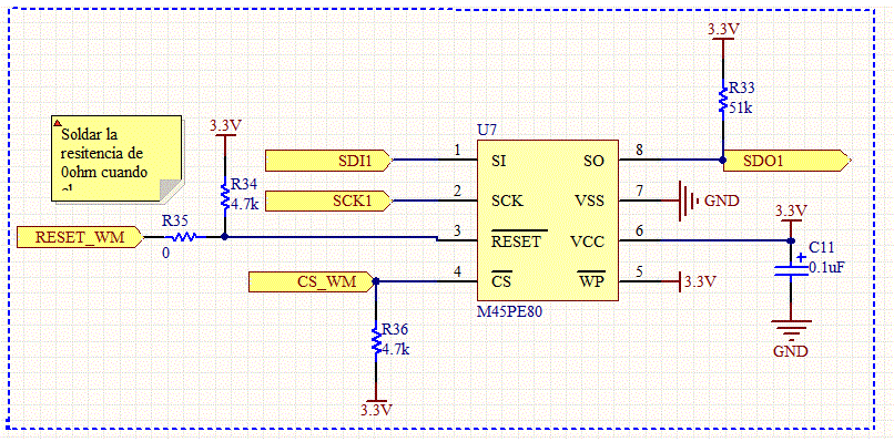
This is the side of the memory: And this is the side of the microcontroler
  So you are telling me that I should use every pin as a Push Pull, and what do you mean with the confusion in the Chip Select?, I hope you help me.
- Mark as New
- Bookmark
- Subscribe
- Mute
- Subscribe to RSS Feed
- Permalink
- Email to a Friend
- Report Inappropriate Content
2013-11-25 09:01 AM
The STM32 is the MASTER you have SDI / SDO wired backward
MOSI = MASTER OUT SLAVE IN MISO = MASTER IN SLAVE OUT LOW = ZERO = RESET HIGH = VCC = SETUp vote any posts that you find helpful, it shows what's working..
- Mark as New
- Bookmark
- Subscribe
- Mute
- Subscribe to RSS Feed
- Permalink
- Email to a Friend
- Report Inappropriate Content
2013-11-25 09:27 AM
Oh !!! Big mistake...
I didn't realize that.. But does it response my question about the CLK?- Mark as New
- Bookmark
- Subscribe
- Mute
- Subscribe to RSS Feed
- Permalink
- Email to a Friend
- Report Inappropriate Content
2013-11-25 09:40 AM
But does it response my question about the CLK?
You're inject voltages into the output of the STM32? Do you think that might impact the IO ring supply? Try removing the serial flash and see if the clock pin behaves the same, or if the bandwidth of your scope/probe is appropriate. The chip select is active low, reset the pin to achieve that.Up vote any posts that you find helpful, it shows what's working..
- Mark as New
- Bookmark
- Subscribe
- Mute
- Subscribe to RSS Feed
- Permalink
- Email to a Friend
- Report Inappropriate Content
2013-11-25 11:02 AM
Clive1 you are right,
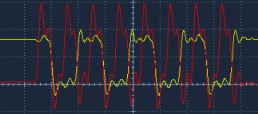
The Signal clock is correct after remove the chip. But I have another question:- As you go faster with the CLK, Should I use a external hardware to ensure the square wave? , because I got this for 42Mhz of frequency:

- Mark as New
- Bookmark
- Subscribe
- Mute
- Subscribe to RSS Feed
- Permalink
- Email to a Friend
- Report Inappropriate Content
2013-11-25 11:46 AM
Are you perhaps using a 1x/10x probe in 1x mode? Check bandwidth of probe/scope.
Up vote any posts that you find helpful, it shows what's working..
- Mark as New
- Bookmark
- Subscribe
- Mute
- Subscribe to RSS Feed
- Permalink
- Email to a Friend
- Report Inappropriate Content
2013-12-03 09:03 AM
Thanks Clive1, you were right again...
The wave was correct ... and everything is right after turn the probe test in x10...
- Mark as New
- Bookmark
- Subscribe
- Mute
- Subscribe to RSS Feed
- Permalink
- Email to a Friend
- Report Inappropriate Content
2013-12-03 10:06 AM
The bandwidth of 1x/10x probes in 1x mode is generally worse than useless.
has done a number of very instructive videos, the kind of stuff you had hoped the professor would have explained a little bit better.http://www.eevblog.com/forum/blog/eevblog-453-mysteries-of-x1-oscilloscope-probes-revealed/
Up vote any posts that you find helpful, it shows what's working..
- usb otg voltage level shifter in STM32 MCUs products
- STM32F429ZIT6 SPI Receive Issue in STM32 MCUs products
- G431RBT6 - Interfacing timer and compare output timer have rather fluctuation timings in STM32 MCUs products
- PWM problems in STM32 MCUs products
- stm32wle5 SMPS oscillates when Vdd ~ 1.7V and prevents power ramp-up in STM32 MCUs Wireless