- STMicroelectronics Community
- STM32 MCUs
- STM32 MCUs products
- [solved] works FSMC correct on stm32f407vg ?
- Subscribe to RSS Feed
- Mark Topic as New
- Mark Topic as Read
- Float this Topic for Current User
- Bookmark
- Subscribe
- Mute
- Printer Friendly Page
[solved] works FSMC correct on stm32f407vg ?
- Mark as New
- Bookmark
- Subscribe
- Mute
- Subscribe to RSS Feed
- Permalink
- Email to a Friend
- Report Inappropriate Content
2014-11-25 02:33 AM
Hi. All!
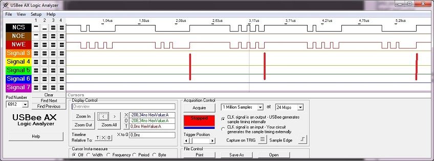
I want to use FSMC module, but I'm not sure that it settings correct. There is write operation on a picture. I see multiple NWE activation. And sometime it release NEx together NWE (should be NWE and than NEx). What should I do for diagram like Figure 437 from ? Or, possible, I don't understand something? Code:
Code:
typedef
struct
{
__IO uint8_t data;
} Modem_TypeDef;
#define MDATA ((uint32_t)(0x60000000))
#define MADDR ((uint32_t)(0x60000000 | 0x100))
#define M_DATA ((Modem_TypeDef *) MDATA)
#define M_ADDR ((Modem_TypeDef *) MADDR)
{
initFSMC();
while
(1)
{
GPIO_WriteBit( GPIOE, GPIO_Pin_0, Bit_SET);
//my own strobe
M_DATA->data = 0x77;
M_ADDR->data = 0x33;
GPIO_WriteBit( GPIOE, GPIO_Pin_0, Bit_RESET);
//my own strobe
}
}
void
initFSMC(
void
)
{
// --- initialization FSMC ---
RCC_AHB1PeriphClockCmd(RCC_AHB1Periph_GPIOD | RCC_AHB1Periph_GPIOE, ENABLE);
//clock for FSMC
RCC_AHB3PeriphClockCmd( RCC_AHB3Periph_FSMC, ENABLE);
// configure GPIOE [4:8]
gpio.GPIO_Mode = GPIO_Mode_AF;
gpio.GPIO_OType = GPIO_OType_PP;
gpio.GPIO_Pin = GPIO_Pin_7 | GPIO_Pin_8 | GPIO_Pin_9 | GPIO_Pin_10 | GPIO_Pin_11;
gpio.GPIO_PuPd = GPIO_PuPd_UP;
gpio.GPIO_Speed = GPIO_Speed_25MHz;
GPIO_Init( GPIOE, &gpio);
// configure GPIOD [0,1,4,5,7,14,15]
gpio.GPIO_Mode = GPIO_Mode_AF;
gpio.GPIO_OType = GPIO_OType_PP;
gpio.GPIO_Pin = GPIO_Pin_0 | GPIO_Pin_1 | GPIO_Pin_4 | GPIO_Pin_5 |\
GPIO_Pin_7 | GPIO_Pin_14 | GPIO_Pin_15;
gpio.GPIO_PuPd = GPIO_PuPd_UP;
gpio.GPIO_Speed = GPIO_Speed_25MHz;
GPIO_Init( GPIOD, &gpio);
// timings
modemTimInit_str.FSMC_AddressSetupTime = 0;
// used but don't care
modemTimInit_str.FSMC_AddressHoldTime = 0;
// don't used
modemTimInit_str.FSMC_DataSetupTime = 5;
modemTimInit_str.FSMC_BusTurnAroundDuration = 0;
// don't used
modemTimInit_str.FSMC_CLKDivision = 2;
modemTimInit_str.FSMC_DataLatency = 0;
// don't used
modemTimInit_str.FSMC_AccessMode = FSMC_AccessMode_A;
FSMC_NORSRAMStructInit( &modemInit_str);
// Apply default values
// Reset NOR/SRAM Initialization structure parameters values
modemInit_str.FSMC_Bank = FSMC_Bank1_NORSRAM1;
modemInit_str.FSMC_DataAddressMux = FSMC_DataAddressMux_Enable;
modemInit_str.FSMC_MemoryType = FSMC_MemoryType_PSRAM;
//FSMC_MemoryType_SRAM;
modemInit_str.FSMC_MemoryDataWidth = FSMC_MemoryDataWidth_8b;
modemInit_str.FSMC_BurstAccessMode = FSMC_BurstAccessMode_Disable;
modemInit_str.FSMC_AsynchronousWait = FSMC_AsynchronousWait_Disable;
modemInit_str.FSMC_WaitSignalPolarity = FSMC_WaitSignalPolarity_Low;
modemInit_str.FSMC_WrapMode = FSMC_WrapMode_Disable;
modemInit_str.FSMC_WaitSignalActive = FSMC_WaitSignalActive_BeforeWaitState;
modemInit_str.FSMC_WriteOperation = FSMC_WriteOperation_Enable;
modemInit_str.FSMC_WaitSignal = FSMC_WaitSignal_Disable;
modemInit_str.FSMC_ExtendedMode = FSMC_ExtendedMode_Enable;
//FSMC_ExtendedMode_Disable;
modemInit_str.FSMC_WriteBurst = FSMC_WriteBurst_Disable;
modemInit_str.FSMC_ReadWriteTimingStruct = &modemTimInit_str;
modemInit_str.FSMC_WriteTimingStruct = &modemTimInit_str;
GPIO_PinAFConfig(GPIOE, GPIO_PinSource7, GPIO_AF_FSMC);
GPIO_PinAFConfig(GPIOE, GPIO_PinSource8, GPIO_AF_FSMC);
GPIO_PinAFConfig(GPIOE, GPIO_PinSource9, GPIO_AF_FSMC);
GPIO_PinAFConfig(GPIOE, GPIO_PinSource10, GPIO_AF_FSMC);
GPIO_PinAFConfig(GPIOE, GPIO_PinSource11, GPIO_AF_FSMC);
GPIO_PinAFConfig(GPIOD, GPIO_PinSource0, GPIO_AF_FSMC);
GPIO_PinAFConfig(GPIOD, GPIO_PinSource1, GPIO_AF_FSMC);
GPIO_PinAFConfig(GPIOD, GPIO_PinSource4, GPIO_AF_FSMC);
GPIO_PinAFConfig(GPIOD, GPIO_PinSource5, GPIO_AF_FSMC);
GPIO_PinAFConfig(GPIOD, GPIO_PinSource7, GPIO_AF_FSMC);
GPIO_PinAFConfig(GPIOD, GPIO_PinSource14, GPIO_AF_FSMC);
GPIO_PinAFConfig(GPIOD, GPIO_PinSource15, GPIO_AF_FSMC);
FSMC_NORSRAMInit( &modemInit_str);
FSMC_NORSRAMCmd( FSMC_Bank1_NORSRAM1, ENABLE);
}- Labels:
-
FMC-FSMC
-
STM32F4 Series
- Mark as New
- Bookmark
- Subscribe
- Mute
- Subscribe to RSS Feed
- Permalink
- Email to a Friend
- Report Inappropriate Content
2014-11-25 10:19 AM
At 24 Msamples per second you are probably not capturing single write pulses - if you run the mcu at 168MHz, they should last around 40ns. Show us also the capture of your ''marker'' signal, not hand-drawn lines.
Also, I don't speak the library gobbledygook, but it appears to me that you set FSMC for multiplexed memory but you don't initialize FSMC_NL, I suspect you do this in error. JW- Mark as New
- Bookmark
- Subscribe
- Mute
- Subscribe to RSS Feed
- Permalink
- Email to a Friend
- Report Inappropriate Content
2014-11-25 06:55 PM
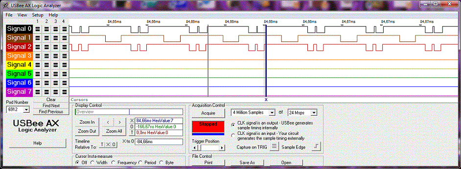
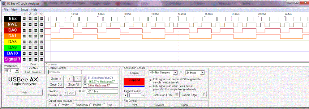
Thank you! You was right - samplerate was too low. It worked on default frequency - 16MHz HSI (not 168MHz, of course! ), but samples couldn't show all details. For 16MHz need 32MHz sample frequency minimum (as told Nyqist and Kotelnikov).
I addedRCC_HCLKConfig( RCC_SYSCLK_Div4);
// make it slow
and now I have this one. Black - NEx,red
- NWE,brown
- soft strobe (see source upper): Also, I don't speak the library gobbledygook, Hah! I can do the same over registers, but library (SPL) do writing code simplier and help me study new MCU faster. Possible, code using library isn't readable for you - sorry. but it appears to me that you set FSMC for multiplexed memory but you don't initialize FSMC_NL, I suspect you do this in error. Can you explain it more detail? What means 'multiplexed' for FSMC? In my appinion, it means that data and address used the same wires. No? Not only? When need FSMC_NL signal? I don't need it really. But ,if FSMC_NL can separate address and data - it will be great! Now I want to use just A8 bit.
- Mark as New
- Bookmark
- Subscribe
- Mute
- Subscribe to RSS Feed
- Permalink
- Email to a Friend
- Report Inappropriate Content
2014-11-26 10:29 AM
> now I have this one
And what's wrong with it?
> Can you explain it more detail? What means 'multiplexed' for FSMC? In my appinion, it means that data and address used the same wires. Roughly, yes. So, you need some way to distinguish between data and address. That is the purpose of FSMC_NL - it is supposed to drive a latch which latches the addresses before data are read/written. Read the manual. > I don't need it really. Now I want to use just A8 bit. Then don't use the multiplexing mode. JW
- Mark as New
- Bookmark
- Subscribe
- Mute
- Subscribe to RSS Feed
- Permalink
- Email to a Friend
- Report Inappropriate Content
2014-11-26 11:54 PM
I can't do it still! Agrh...
So, I need ModeA or ModeD. It means, I should use extended mode and write timings in both BTR1 and BWTR1 ( bank 1 for NOR/PSRAM). I declare structure for IO:#define
M_BASE ((uint32_t)(0x60000000))#define
MADDR ((uint32_t)((0x60000000 | 0x100)-4))#define
M_ADDR ((Modem_TypeDef *) MADDR) So, now I can write there:for (i=0;i<8;i++) {
M_ADDR->data[i] = i; } and listing:80004a8: 2300 movs r3, #0
for (i=0;i<8;i++) { M_ADDR->data[i] = i; 80004aa: 4a07 ldr r2, [pc, #28] ; (80004c8 <main+0x88>) 80004ac: b2d9 uxtb r1, r3 80004ae: 54d1 strb r1, [r2, r3] 80004b0: 3301 adds r3, #1 for (i=0;i<8;i++) { 80004b2: 2b08 cmp r3, #8 80004b4: d1f9 bne.n 80004aa <main+0x6a> 80004b6: e7ef b.n 8000498 <main+0x58> 80004c8: 600000fc .word 0x600000fc For use this opportunity request initialize FSMC module: clock, gpio, connect pins to alternate function.void
initFSMC(
void
)
{
FSMC_NORSRAMInitTypeDef modemInit_str;
FSMC_NORSRAMTimingInitTypeDef modemTimings;
// --- initialization FSMC ---
RCC_AHB1PeriphClockCmd(RCC_AHB1Periph_GPIOD | RCC_AHB1Periph_GPIOE | RCC_AHB1Periph_GPIOB, ENABLE);
//clock for FSMC
RCC_AHB3PeriphClockCmd( RCC_AHB3Periph_FSMC, ENABLE);
GPIO_PinAFConfig(GPIOE, GPIO_PinSource7, GPIO_AF_FSMC);
GPIO_PinAFConfig(GPIOE, GPIO_PinSource8, GPIO_AF_FSMC);
GPIO_PinAFConfig(GPIOE, GPIO_PinSource9, GPIO_AF_FSMC);
GPIO_PinAFConfig(GPIOE, GPIO_PinSource10, GPIO_AF_FSMC);
GPIO_PinAFConfig(GPIOE, GPIO_PinSource11, GPIO_AF_FSMC);
GPIO_PinAFConfig(GPIOE, GPIO_PinSource12, GPIO_AF_FSMC);
GPIO_PinAFConfig(GPIOE, GPIO_PinSource13, GPIO_AF_FSMC);
GPIO_PinAFConfig(GPIOE, GPIO_PinSource14, GPIO_AF_FSMC);
GPIO_PinAFConfig(GPIOE, GPIO_PinSource15, GPIO_AF_FSMC);
GPIO_PinAFConfig(GPIOD, GPIO_PinSource0, GPIO_AF_FSMC);
GPIO_PinAFConfig(GPIOD, GPIO_PinSource1, GPIO_AF_FSMC);
GPIO_PinAFConfig(GPIOD, GPIO_PinSource4, GPIO_AF_FSMC);
GPIO_PinAFConfig(GPIOD, GPIO_PinSource5, GPIO_AF_FSMC);
GPIO_PinAFConfig(GPIOD, GPIO_PinSource7, GPIO_AF_FSMC);
GPIO_PinAFConfig(GPIOD, GPIO_PinSource14, GPIO_AF_FSMC);
GPIO_PinAFConfig(GPIOD, GPIO_PinSource15, GPIO_AF_FSMC);
GPIO_PinAFConfig(GPIOD, GPIO_PinSource8, GPIO_AF_FSMC);
GPIO_PinAFConfig(GPIOD, GPIO_PinSource9, GPIO_AF_FSMC);
GPIO_PinAFConfig(GPIOD, GPIO_PinSource10, GPIO_AF_FSMC);
GPIO_PinAFConfig(GPIOB, GPIO_PinSource7, GPIO_AF_FSMC);
// configure GPIOE [4:8]
gpio.GPIO_Mode = GPIO_Mode_AF;
gpio.GPIO_OType = GPIO_OType_PP;
//gpio.GPIO_Pin = GPIO_Pin_7 | GPIO_Pin_8 | GPIO_Pin_9 | GPIO_Pin_10 | GPIO_Pin_11;
gpio.GPIO_Pin = GPIO_Pin_7 | GPIO_Pin_8 | GPIO_Pin_9 | GPIO_Pin_10 | GPIO_Pin_11 | GPIO_Pin_12 | \
GPIO_Pin_13 | GPIO_Pin_14 | GPIO_Pin_15;
gpio.GPIO_PuPd = GPIO_PuPd_UP;
gpio.GPIO_Speed = GPIO_Speed_25MHz;
GPIO_Init( GPIOE, &gpio);
// configure GPIOD [0,1,4,5,7,14,15]
gpio.GPIO_Mode = GPIO_Mode_AF;
gpio.GPIO_OType = GPIO_OType_PP;
//gpio.GPIO_Pin = GPIO_Pin_0 | GPIO_Pin_1 | GPIO_Pin_4 | GPIO_Pin_5 | GPIO_Pin_7 | GPIO_Pin_14 | GPIO_Pin_15;
gpio.GPIO_Pin = GPIO_Pin_0 | GPIO_Pin_1 | GPIO_Pin_4 | GPIO_Pin_5 | GPIO_Pin_7 | GPIO_Pin_14 | GPIO_Pin_15 | \
GPIO_Pin_8 | GPIO_Pin_9 | GPIO_Pin_10;
gpio.GPIO_PuPd = GPIO_PuPd_UP;
gpio.GPIO_Speed = GPIO_Speed_25MHz;
GPIO_Init( GPIOD, &gpio);
// configure GPIOB [7]
gpio.GPIO_Mode = GPIO_Mode_AF;
gpio.GPIO_OType = GPIO_OType_PP;
gpio.GPIO_Pin = GPIO_Pin_7;
gpio.GPIO_PuPd = GPIO_PuPd_UP;
gpio.GPIO_Speed = GPIO_Speed_25MHz;
GPIO_Init( GPIOB, &gpio);
// over Register
// Timings MODE A
//ACCMOD BUSTURN DATAST ADDHLD
// || |||| | | | | ADDSET
// 33 22 2222 2222 1111 111111 | | |
// 10 98 7654 3210 9876 54321098 7654 3210
// oo 00 oooo oooo 0000 00000101 oooo 0011 BTR1,BWTR=0x00000503
FSMC_Bank1E->BWTR[0]=(uint32_t) 0x0503;
//WriteMode timings
FSMC_Bank1->BTCR[1]=(uint32_t) 0x0503;
//ReadMode timings
// EXTMOD WREN MTYP[SRAM|PSRAM|NOR]
// | | MWID[8|16] || MUXEN
// 332222222222 1 111 1 1 1 1 1 1 || || | MBKEN
// 109876543210 9 876 5 4 3 2 1 0 9 8 7 6 54 32 1 0
// oooooooooooo.0 000.0 1 0 1.o 0 o 0.l o 00.01 0 1 BCR1=0x0000 5085
FSMC_Bank1->BTCR[0]=(uint32_t) 0x5085;
} I want to connect 8bit devise just. Why is it so difficult?

- Mark as New
- Bookmark
- Subscribe
- Mute
- Subscribe to RSS Feed
- Permalink
- Email to a Friend
- Report Inappropriate Content
2014-11-27 05:53 AM
People, who have english as native language, please, check details in Table 218 on RM0090 and explain me - can I use SRAM/PSRAM in 8 bit read-write mode?
- Mark as New
- Bookmark
- Subscribe
- Mute
- Subscribe to RSS Feed
- Permalink
- Email to a Friend
- Report Inappropriate Content
2014-11-27 10:30 AM
That has nothing to do with English; it's simply a prime example of the inferior quality of STM32 documentation.
Note, that that table's title is ''example of supported memories and transactions''. I guess it comes from some preliminary internal/promo material to the FSMC IP module, and IMO it should've never appeared in the manual, and serves only to confusion. Of course you can use 8-bit SRAM. JW- Mark as New
- Bookmark
- Subscribe
- Mute
- Subscribe to RSS Feed
- Permalink
- Email to a Friend
- Report Inappropriate Content
2014-11-27 07:18 PM
Thank you, Jan.
I asked about ''Memory data width'' column - what it means? Why is it always 16? Should I use only 16bit SRAM? Or I should separate low and high byte over NBL? One more moment - I forgot check some details in datasheet. 407VG hasn't lower adress lines, because it hasn't port F and G. Sorry... I agree - ST document style isn't easy to understand. For example - TI is better. But their chip is more expensive (for me only, maybe).- Mark as New
- Bookmark
- Subscribe
- Mute
- Subscribe to RSS Feed
- Permalink
- Email to a Friend
- Report Inappropriate Content
2014-11-27 11:38 PM
So, how to connect 8bit device like SRAM?
Firstly, see a Table ''FSMC pin definition''. I didn't do it at first - it was my mistake. If your chip hasn't some pin - you can't use these signals. For 407VG and SRAM you hasn't address line A[15:0]. Initialise requested pins D[7:0], NEx, NOE, NWE A[max:16] and other if you need as described in ''stm32f4xx_fsmc.c'' (strange place, imho). And when you write or read your device - you should calculate address as MEMBASE+(ADDR<<n), where MEMBASE = 0x60000000 for SRAM/PSRAM/NOR bank, ADDR = byte's address in your device, n =17. b.r., Oleg- Setting up HyperRAM S70KL1282 with STM32H735 issues in STM32 MCUs products
- STM32U5A5: PSRAM (4MB external RAM) via QSPI (OCTOSPI1) - for you in STM32 MCUs products
- How to use HAL_UART_Receive_IT to receive uart data? in STM32 MCUs products
- ST7701 (Video mode) printing framebuffer differently in STM32 MCUs TouchGFX and GUI
- MCSDK 6.2 and IHM042-V1 Dual Motor Position Control in STM32 MCUs Motor control