- STMicroelectronics Community
- STM32 MCUs
- STM32 MCUs products
- STM32F7 FMC SRAM problems
- Subscribe to RSS Feed
- Mark Topic as New
- Mark Topic as Read
- Float this Topic for Current User
- Bookmark
- Subscribe
- Mute
- Printer Friendly Page
STM32F7 FMC SRAM problems
- Mark as New
- Bookmark
- Subscribe
- Mute
- Subscribe to RSS Feed
- Permalink
- Email to a Friend
- Report Inappropriate Content
2016-06-02 06:24 AM
Hi All,
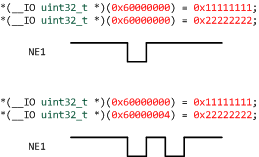
The device is being used STM32F746BGTX.Set as follows. FMC_NORSRAM_TimingTypeDef Timing; /** Perform the SRAM1 memory initialization sequence */ hsram1.Instance = FMC_NORSRAM_DEVICE; hsram1.Extended = FMC_NORSRAM_EXTENDED_DEVICE; /* hsram1.Init */ hsram1.Init.NSBank = FMC_NORSRAM_BANK1; hsram1.Init.DataAddressMux = FMC_DATA_ADDRESS_MUX_DISABLE; hsram1.Init.MemoryType = FMC_MEMORY_TYPE_SRAM; hsram1.Init.MemoryDataWidth = FMC_NORSRAM_MEM_BUS_WIDTH_32; hsram1.Init.BurstAccessMode = FMC_BURST_ACCESS_MODE_DISABLE; hsram1.Init.WaitSignalPolarity = FMC_WAIT_SIGNAL_POLARITY_LOW; hsram1.Init.WaitSignalActive = FMC_WAIT_TIMING_BEFORE_WS; hsram1.Init.WriteOperation = FMC_WRITE_OPERATION_ENABLE; hsram1.Init.WaitSignal = FMC_WAIT_SIGNAL_DISABLE; hsram1.Init.ExtendedMode = FMC_EXTENDED_MODE_DISABLE; hsram1.Init.AsynchronousWait = FMC_ASYNCHRONOUS_WAIT_DISABLE; hsram1.Init.WriteBurst = FMC_WRITE_BURST_DISABLE; hsram1.Init.ContinuousClock = FMC_CONTINUOUS_CLOCK_SYNC_ONLY; hsram1.Init.WriteFifo = FMC_WRITE_FIFO_DISABLE; hsram1.Init.PageSize = FMC_PAGE_SIZE_NONE; /* Timing */ Timing.AddressSetupTime = 0; Timing.AddressHoldTime = 15; Timing.DataSetupTime = 1; Timing.BusTurnAroundDuration = 0; Timing.CLKDivision = 16; Timing.DataLatency = 17; Timing.AccessMode = FMC_ACCESS_MODE_A; /* ExtTiming */ HAL_SRAM_Init(&hsram1, &Timing, NULL);And when I tried to write multiple times to the same address to write NE1 does not work only once.ex)*(volatile uint32_t *)(0x60000000) = 0x11223344; <- pass*(volatile uint32_t *)(0x60000000) = 0x55667788; <- failWriting to the address other works properly.ex)*(volatile uint32_t *)(0x60000000) = 0x11223344; <- pass*(volatile uint32_t *)(0x60000004) = 0x55667788; <- passIs there a cache problem? Noncache to be the NE1 zone there any?I tried to change it as well as the optimization options.What's the problem?Thank you.
Best regards,gyosun.
- Mark as New
- Bookmark
- Subscribe
- Mute
- Subscribe to RSS Feed
- Permalink
- Email to a Friend
- Report Inappropriate Content
2016-06-02 11:47 AM
The 0x60000000-starting area is cached, write back, by default. You could either disable the cache for that are in the MMU, or swap the FMC's ''NOR'' area for the area starting at 0xC0000000 using SYSCFG_MEMRMP.SWP_FMC. See AN4839, PM0253, and RM0385 of course.
JW- Mark as New
- Bookmark
- Subscribe
- Mute
- Subscribe to RSS Feed
- Permalink
- Email to a Friend
- Report Inappropriate Content
2016-06-02 09:22 PM
Thank you for answer.
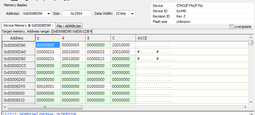
RM0385 Manual was set to see the MPU_RASR register as shown below. Still, there are following problems.
 cache was also disable.SCB_DisableICache();SCB_DisableDCache();What's the problem?Also compiler option problems?Add to this the gap between NE1 NE1 too large. About 1us?----__--__----NE1 is about 140ns.FMC_BCR1 register value is 0x002010A1.FMC_BTR1 register value is 0x0FF001F0.
Thank you.
Best regards,gyosun.
- Mark as New
- Bookmark
- Subscribe
- Mute
- Subscribe to RSS Feed
- Permalink
- Email to a Friend
- Report Inappropriate Content
2016-06-03 12:35 AM
Well, the answer is still ''I don't know'', but try also my other suggestion - the remap to 0xC0000000. The rationale behind this suggestion lies beyond the cache in the ''Device'' vs. ''Memory'' type of the two areas - the processor itself is allowed to merge accesses in ''Memory'' area.
JW- Mark as New
- Bookmark
- Subscribe
- Mute
- Subscribe to RSS Feed
- Permalink
- Email to a Friend
- Report Inappropriate Content
2016-06-03 01:19 AM
gyosun, your problem is related to ARM architecture.
The region at 0x60000000 is defined as memory region, so it can use caches and (most important) write buffer. That last can merge and coalesce writes to the memory, this is exactly what happens to you. There are (at least) 2 solutions: 1) declare the region as Device or Strongly ordered, by reprogramming the MPU (don't trust your screen capture, MPU_RASR is a port, and currently related to a 128KB region starting at 0x20010000, according values in both MPU_RBAR and MPU_RASR). 2) use memory barriers instructions between your accesses (DMB/DSB, see the manual to understand difference between them). BTW, if there is memory behing 0x60000000, I will expect that merge or coalescing is not harmfull. What is the use case where writing twice the same memory area is absolutely required ?- Mark as New
- Bookmark
- Subscribe
- Mute
- Subscribe to RSS Feed
- Permalink
- Email to a Friend
- Report Inappropriate Content
2016-06-09 05:22 AM
Thanks all,
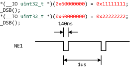
When you write, as shown below and run the _DSB () function, even if the write to the same address works fine.But the gap between chip select is too large. read also the same.Is there any way to further reduce? Or Is it structurally impossible to?
Thank you.
Best regards,gyosun.
- Mark as New
- Bookmark
- Subscribe
- Mute
- Subscribe to RSS Feed
- Permalink
- Email to a Friend
- Report Inappropriate Content
2016-06-09 06:05 AM
Well, it's just the third time I write it: try the remap.
JW- Mark as New
- Bookmark
- Subscribe
- Mute
- Subscribe to RSS Feed
- Permalink
- Email to a Friend
- Report Inappropriate Content
2016-06-09 06:47 PM
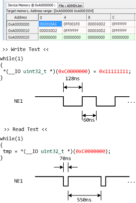
Write to the memory swap as follows seems well out the way you want.
But reading is still too big a chip select intervals.Is there any way to further reduce?
Thank you.
Best regards,gyosun.
- Mark as New
- Bookmark
- Subscribe
- Mute
- Subscribe to RSS Feed
- Permalink
- Email to a Friend
- Report Inappropriate Content
2016-06-09 11:53 PM
Your system clock appears to be the default 16MHz HSI, isn't it. Thus, there are about 9 cycles between the consecutive reads. That is about the maximum you can squeeze out from the processor.
Depending on your particular application, you might be better off using DMA. In that case you don't need to be concerned about cache and device/memory areas, as those relate only to the processor. If you want to get close to the possible extremums, you need to do a lot of manual reading and experimentation to get the knack. JW- Mark as New
- Bookmark
- Subscribe
- Mute
- Subscribe to RSS Feed
- Permalink
- Email to a Friend
- Report Inappropriate Content
2016-06-13 05:41 AM
Thanks JW.
Spoken has been resolved by changing the HCLK clock to 216MHz, as the problem is completely.Thank you.
Best regards,gyosun.
- Interfacing with memory mapped device (i.e. FPGA) on STM32F7 FMC bus in STM32 MCUs products
- Problems with ST7789 LCD code (MCD Application Team) in STM32 MCUs Embedded software
- Strange Behaviors on PA0 Encoder Timer Input on NUCLEO H743ZI2 in STM32 MCUs products
- Connecting eMMC to SDMMC1 on the STM32H7 in STM32 MCUs products
- High current draw Vbat Bluepill in STM32 MCUs products